

Semiconductor memory device capable of correcting a read level properly
a memory device and memory technology, applied in the field of semiconductor memory devices, can solve the problems of difficult to determine the appropriate correction value, the effect of capacity coupling between the floating gates of a plurality of adjacent cells,
- Summary
- Abstract
- Description
- Claims
- Application Information
AI Technical Summary
Benefits of technology
Problems solved by technology
Method used
Image

Examples
first embodiment
[0079] As shown in FIG. 6, for example, when the data is read from cell MC11 in a first embodiment of the invention, first the threshold voltage (also referred to as the threshold level) of the data in cell MC12 written into later than cell MC11 is checked and the value read from cell MC11 at a read level corresponding to the threshold level is determined to be the read-out data from cell MC11.
[0080] As shown in FIG. 7A, first data is written into cell MC11. Thereafter, as shown in FIG. 7B, before adjacent cell MC12 is written into, that is, when the adjacent cell is at the erase level, the data read at read levels AR, BR, CR is the read-out data from cell MC11.
[0081] Moreover, as shown in FIG. 7C, for example, if the adjacent cell is written into from erase level E to level A, the threshold level should have fluctuated because of the capacitance between floating gates. For this reason, shift values DA1, DB1, DC1 are added to the read levels AR, BR, CR, respectively, producing lev...
second embodiment
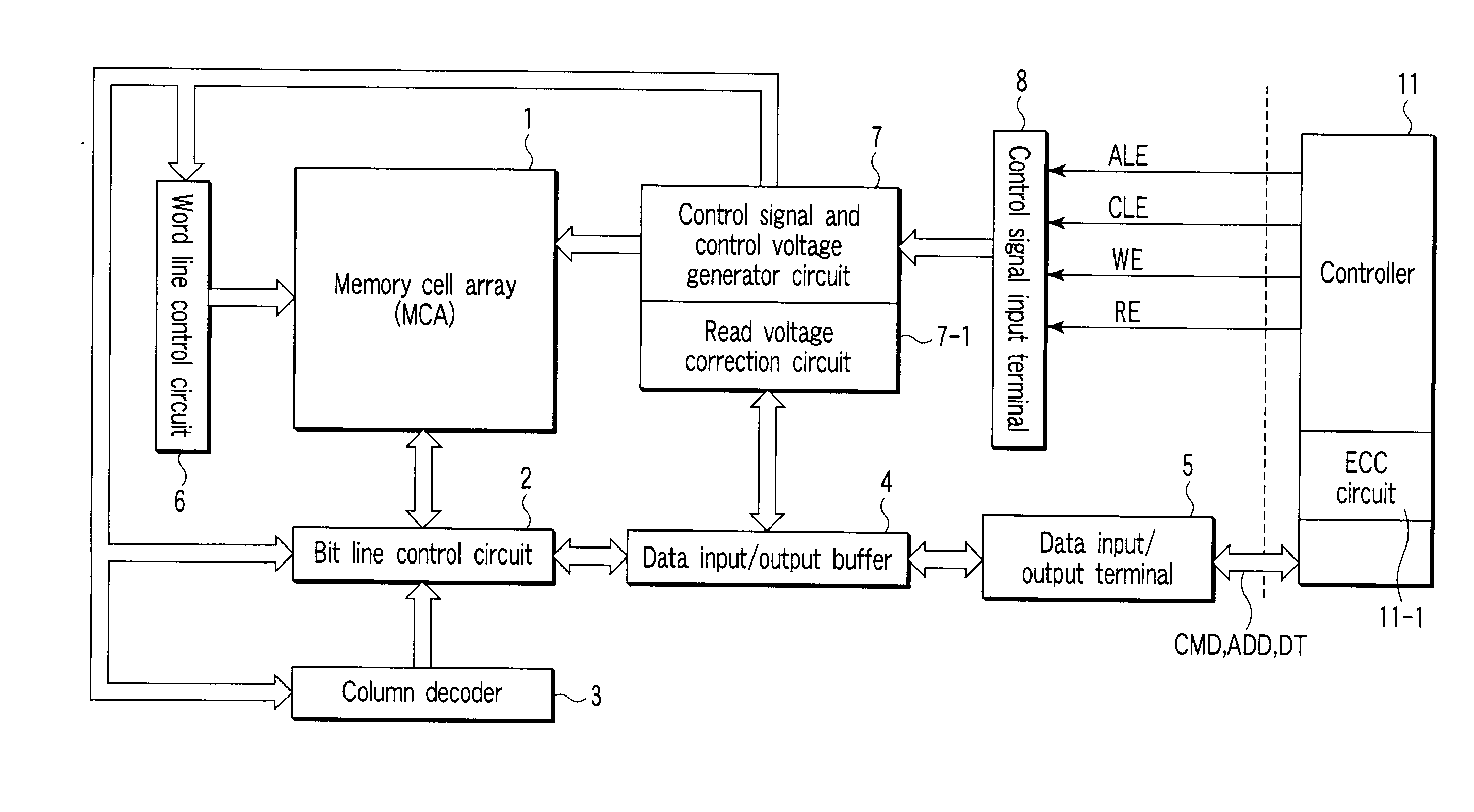
[0097]FIG. 11 shows a second embodiment of the invention. In the first embodiment, the shift values D1, D2, and D3 have been trimmed word line by word line for each chip and these shift values D1, D2, and D3 have been stored as parameters into the storage circuits 71, 72, and 73. In contrast, in the second embodiment, monitor cells are provide in the memory cell array 1, monitor levels are set in the monitor cells, and the read levels of the individual memory cells are determined according to the monitor levels.
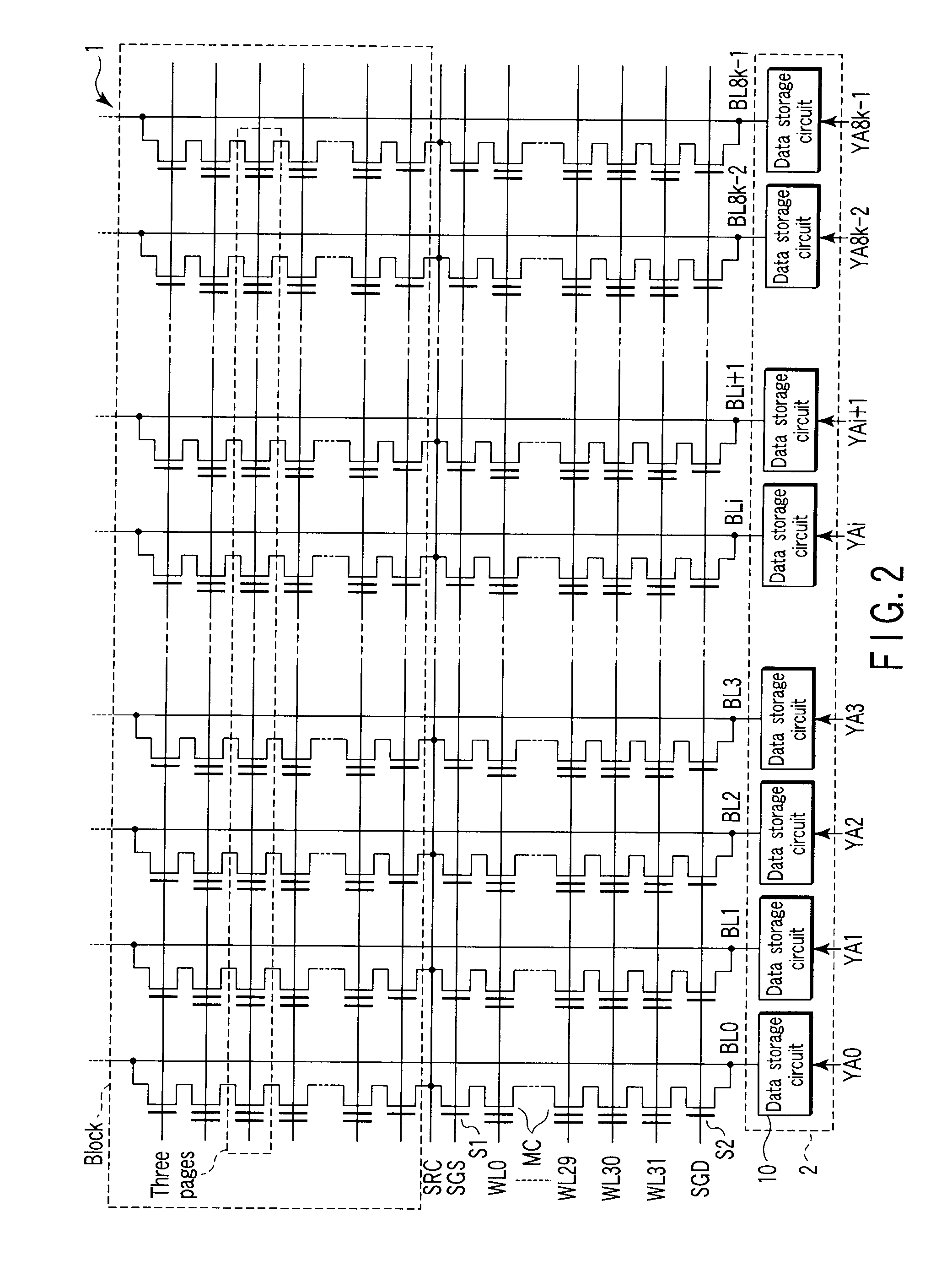
[0098] Specifically, as shown in FIG. 11, the memory cell array 1 includes, for example, a plurality of monitor cells MMC0. The monitor cells MMC0 are connected to, for example, bit line BL-M0. Bit line BL-M0 is connected to each of the data storage circuits 10 and supplied with monitor cell address YA-M0. The monitor cell MMC0 is selected by the address YA-M0 and row address. That is, the monitor cell MMC0 is selected at the same time when the memory cell sharing a word lin...
third embodiment
[0108] FIGS. 14 to 17 show a third embodiment of the invention.
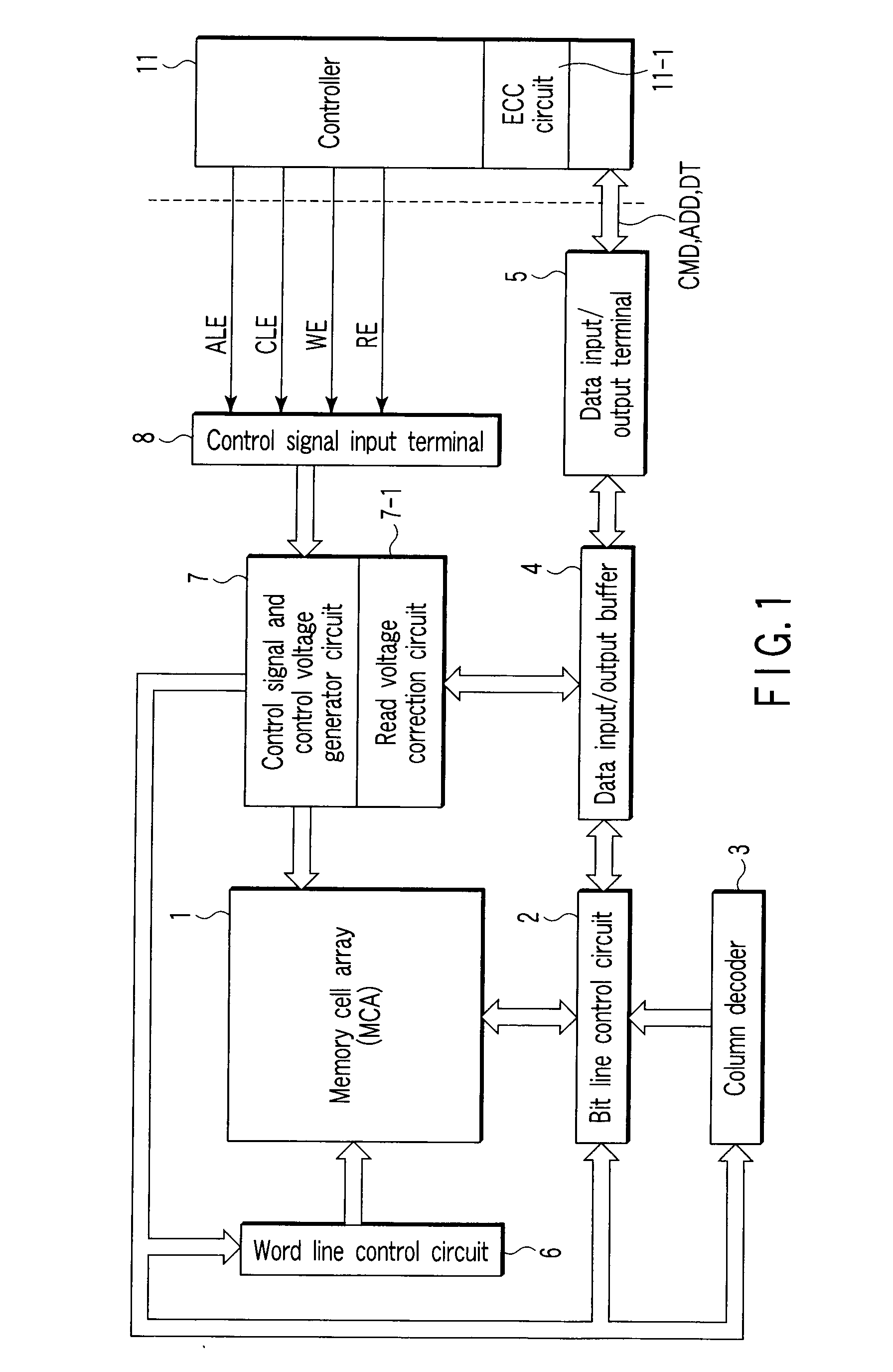
[0109] As described above, in the NAND flash memory, 2 KB (B: bytes) of data are simultaneously written into or read from all of or half of the cells arranged in the row direction. If the threshold level of the cell already written into has changed due to the effect of erroneous writing or the writing of adjacent cells, the accuracy of read-out data can decrease. To increase the accuracy of data, for example, 64-B ECC (Error Correction Code) code is added to 2-KB data, producing (2 KB+64 B) of data, which is written or read.
[0110] For this reason, for example, an ECC circuit 11-1 is provided in the controller 11. The ECC circuit 11-1 is designed to correct an error and output correct data, if incorrect data has been read from a memory cell. The ECC circuit 11-1 may be provided not only in the controller 11 but also in, for example, the NAND flash memory.
[0111] As the ECC code, for example, the BCH code used in correct...
PUM
 Abstract
Description
Claims
Application Information