Method and system for refreshing a memory device during reading thereof

a memory device and reading technology, applied in the field of memory, can solve the problems of wasting space for storing control information in the structure used to implement the ecc, changing the logical value stored, and retaining data,

Active Publication Date: 2007-12-06
STMICROELECTRONICS SRL
View PDF9 Cites 33 Cited by
  • Summary
  • Abstract
  • Description
  • Claims
  • Application Information

AI Technical Summary

Benefits of technology

[0033]FIG. 5 is a schematic block diagram of a control unit of the memory device that can be used to implement the solution according to an embodiment of the invention;
[0034]FIG. 6 illustrates a circuit scheme of a pulser of the control unit according to an embodiment of

Problems solved by technology

A very critical problem of the memory devices known in the art is their data retention.
In fact, the memory cells are subjected to different electrical stresses during operation of the memory devices; these stresses may cause a partial loss of the electrical charge stored in their floating gates, with an undesired erasure of the memory cells that may even cause a change of the logical values stored therein.
This problem is particular acute in modern memory devices, wherein the memory cells have very thin oxide layers.
Nevertheless, the structures used to implement the ECC involve a considerable waste of space for storing the control information.
Furthermore, the operations required to manipulate the control information slow down operation of the memory device.
For example, it is possible to copy a sector of the memory device onto a volatile memory device, erasing the sector, and then restoring the data from the volatile memory device; how

Method used


Image

  • Method and system for refreshing a memory device during reading thereof
  • Method and system for refreshing a memory device during reading thereof
  • Method and system for refreshing a memory device during reading thereof

Examples


Embodiment Construction

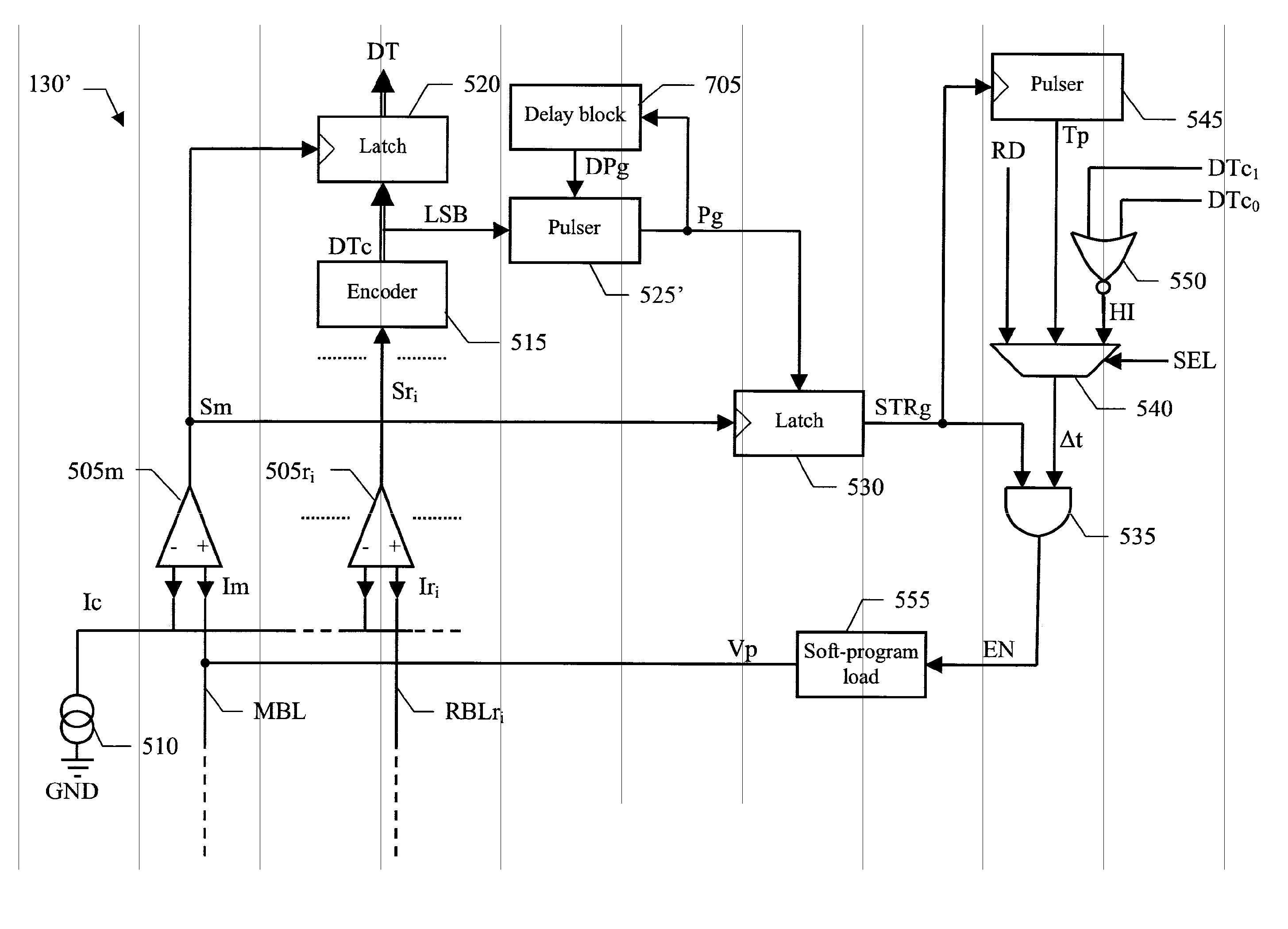
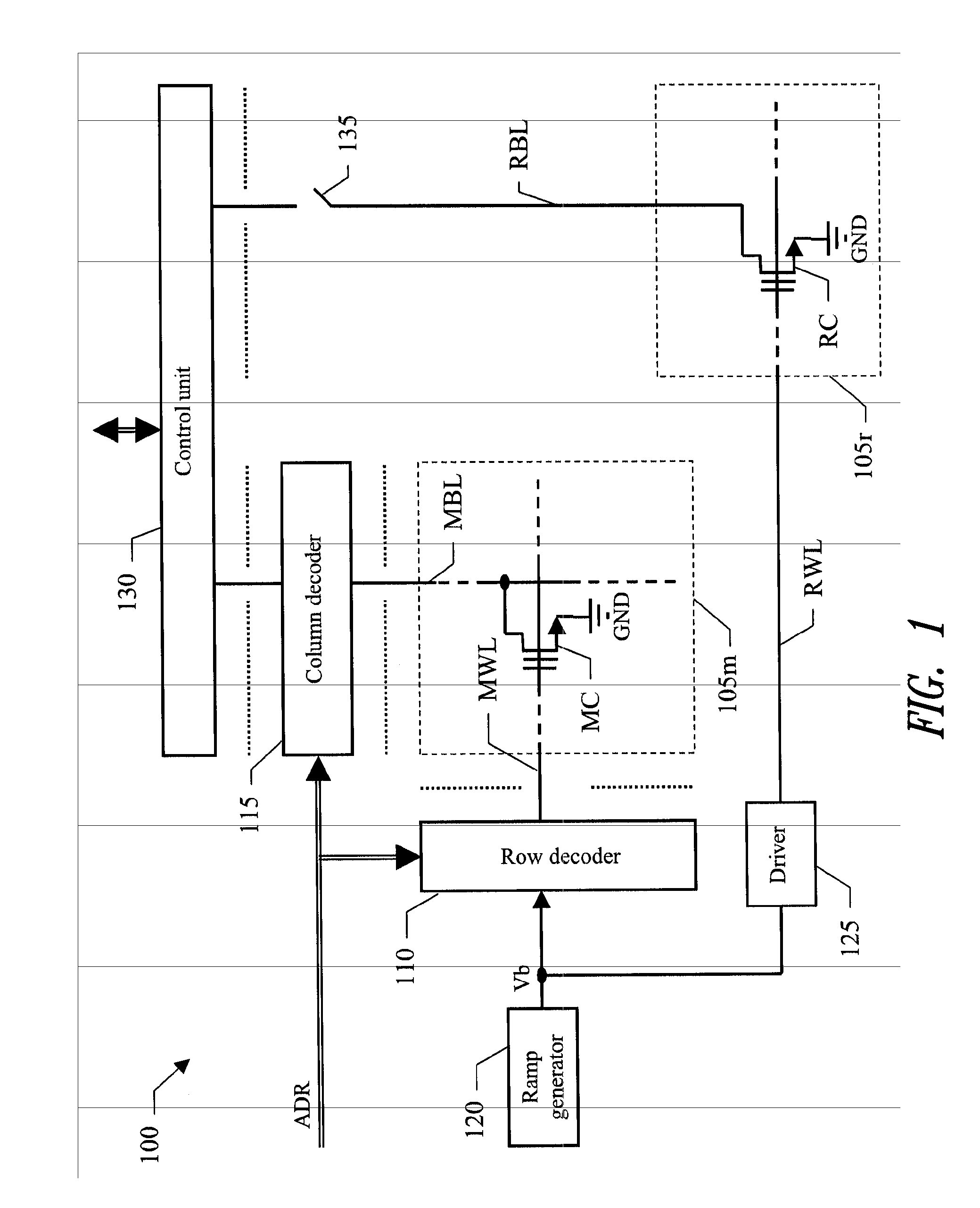
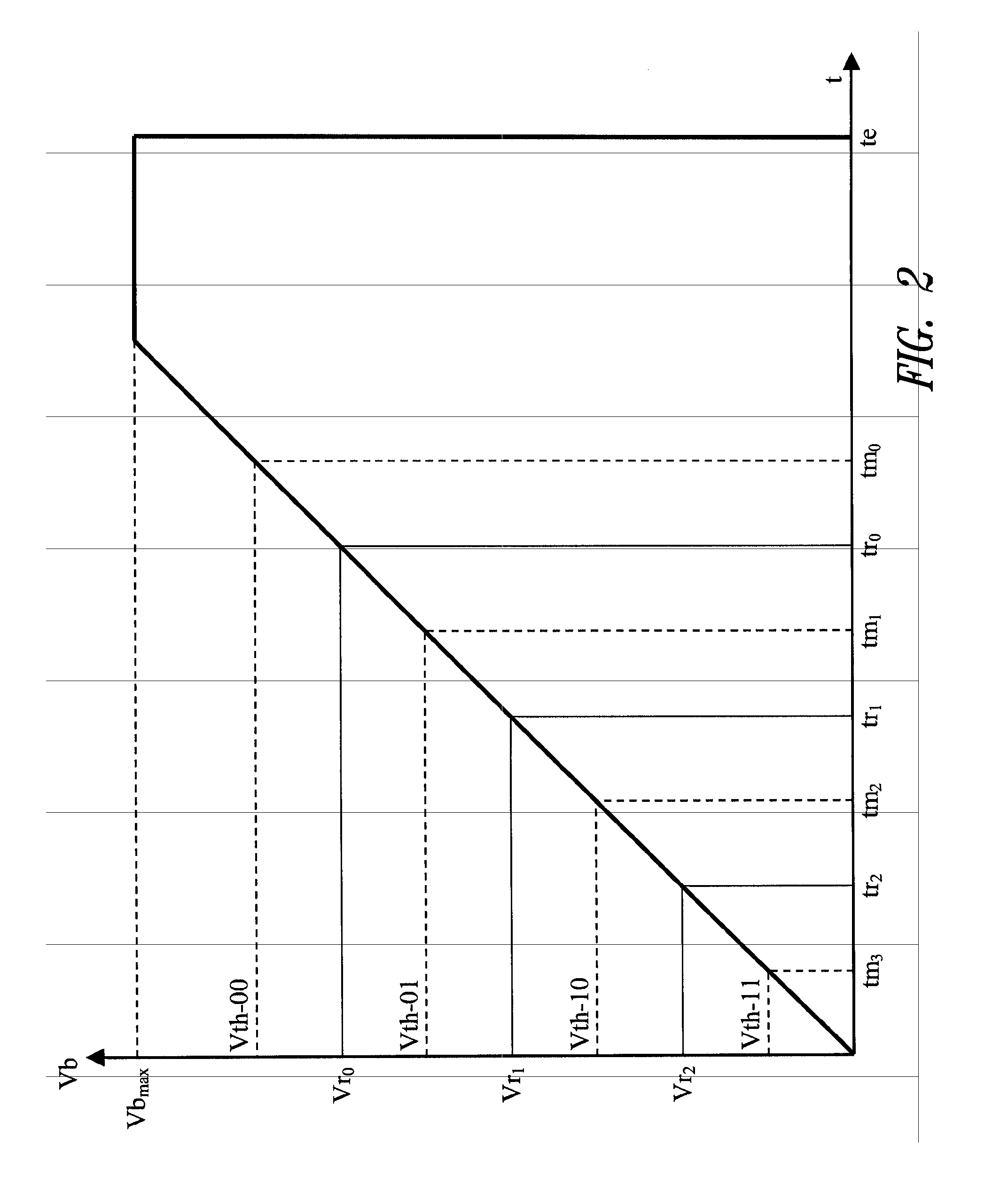
[0037] With reference in particular to FIG. 1, a non-volatile memory device 100 (for example, consisting of a flash E2PROM) is illustrated. The memory device 100 is integrated in a chip of semiconductor material, and includes one or more sectors (only one shown in the figure), each one formed by a matrix 105m of memory cells MC. Each memory cell MC consists of a floating gate MOS transistor with a programmable threshold voltage. The memory cell MC in a non-programmed (or erased) condition exhibits a low threshold voltage. The memory cell MC is programmed by injecting electrical charge into its floating gate; the memory cell MC can be programmed to multiple levels, each one associated with a corresponding range of its threshold voltage. Each level represents a different logical value; for example, the memory device 100 operates at 4 levels, so that each memory cell MC stores a logical value consisting of 2 bits (11, 10, 01 and 00 for increasing threshold voltages). Conversely, the me...


PUM


Abstract

A refresh circuit for refreshing a memory device is proposed. The refresh circuit includes: reading means for reading a set of memory cells, the reading means including means for applying a biasing voltage having a substantially monotone time pattern to the memory cells and to a set of reference cells each one having a reference threshold voltage, means for detecting the reaching of a comparison current by a cell current of each memory cell and by a reference current of each reference cell, and means for determining a condition of each memory cell according to a temporal relation of the reaching of the comparison current by the corresponding cell current and the reference currents, and writing means for applying a writing voltage to at least one selected of the memory cells; the refresh circuit further includes control means for enabling the writing means during at least part of the application of the biasing voltage after the determination of the condition of each selected memory cell.

Description

BACKGROUND OF THE INVENTION [0001] 1. Field of the Invention [0002] The present invention relates to the memory field. More specifically, the present invention relates to the refresh of memory devices. [0003] 2. Description of the Related Art [0004] Memory devices are commonly used to store data in a number of applications; particularly, in a non-volatile memory device the data is preserved even when a power supply is off. Typically, the memory device includes a matrix of memory cells (for example, consisting of floating gate MOS transistors). The memory cells are programmed by injecting electrical charge into their floating gates; conversely, the memory cells are erased by discharging the floating gates. The electrical charge in the floating gate of each memory cell defines different levels of its threshold voltage representing corresponding logical values. Particularly, in a multi-level memory device each memory cell can take more than two levels (and then store a plurality of bit...

Claims


Application Information

Patent Timeline
IPC IPC(8): G11C16/06
CPCG11C16/3418G11C11/5628G11C16/3431
Inventor ROLANDI, PAOLOPASCUCCI, LUIGI
Owner STMICROELECTRONICS SRL
Why Eureka
Try Eureka