Apparatus and method for depositing layer on substrate

Inactive Publication Date: 2007-12-06
SUMCO TECHXIV
View PDF0 Cites 72 Cited by
  • Summary
  • Abstract
  • Description
  • Claims
  • Application Information

AI Technical Summary

Benefits of technology

[0019]According to another and further aspect of the present invention, a method for depositing a layer on a substrate comprises a gas flow step of rotating a substrate and flowing a reactant gas over a surface of the rotating substrate, and a gas flow rate adjustment step of adjusting the gas flow rates of a plurality of gas flow paths for controlling a gas flow velocity distribution laterally across the reactant gas flow. The gas flow rate adjustment step comprises obtaining layer thickness data indicating a thickness of a layer previously deposited by rotation on a substrate whi

Problems solved by technology

As a result, the distribution of the layer on the wafer, that is, the thickness of the layer, becomes uneven (either thinner or thicker) as the reactant gas is consumed.
However, no matter how the gas flow rates of the seven gas transport channels are adjusted there is a limit to the precision of the layer thickness distribution that can be achieved thereby, and it becomes difficult to satisfy the ever more demanding requirement for layer thickness uniformity.
However, if there are too many gas transport channels, a different problem like the following occurs, possibly making uniform layer thickness distr

Method used


Image

  • Apparatus and method for depositing layer on substrate
  • Apparatus and method for depositing layer on substrate
  • Apparatus and method for depositing layer on substrate

Examples


Embodiment Construction

[0040]Preferred embodiments of the present invention will now be described in detail with reference to the accompanying drawings.

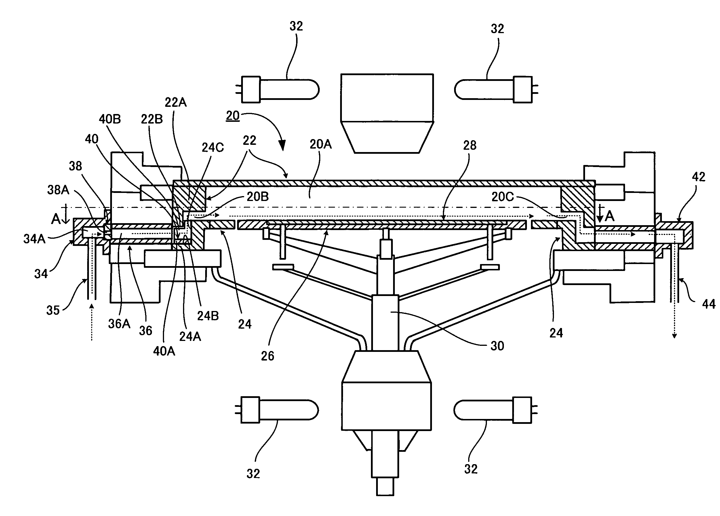
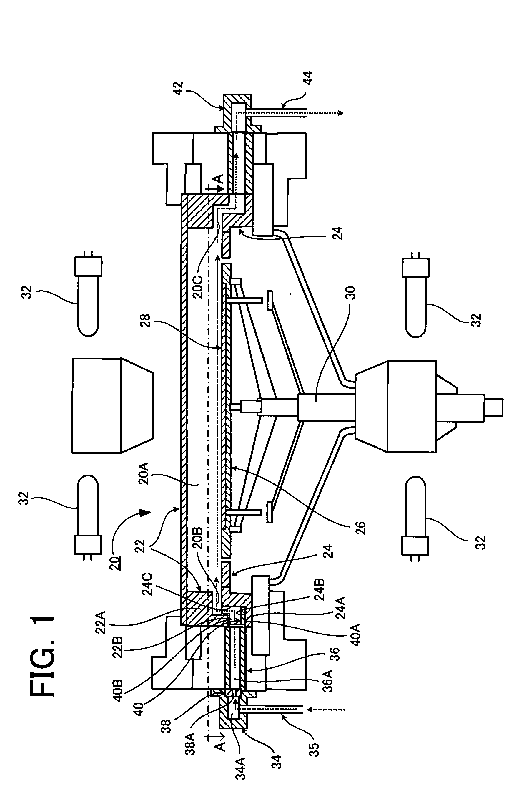
[0041]FIG. 1 is a sectional view of the main components of a layer depositing reactor according to one embodiment of the present invention. This layer depositing reactor can be used to form an epitaxial layer of semiconductive material like silicon on the surface of a semiconductor wafer such as a silicon wafer.

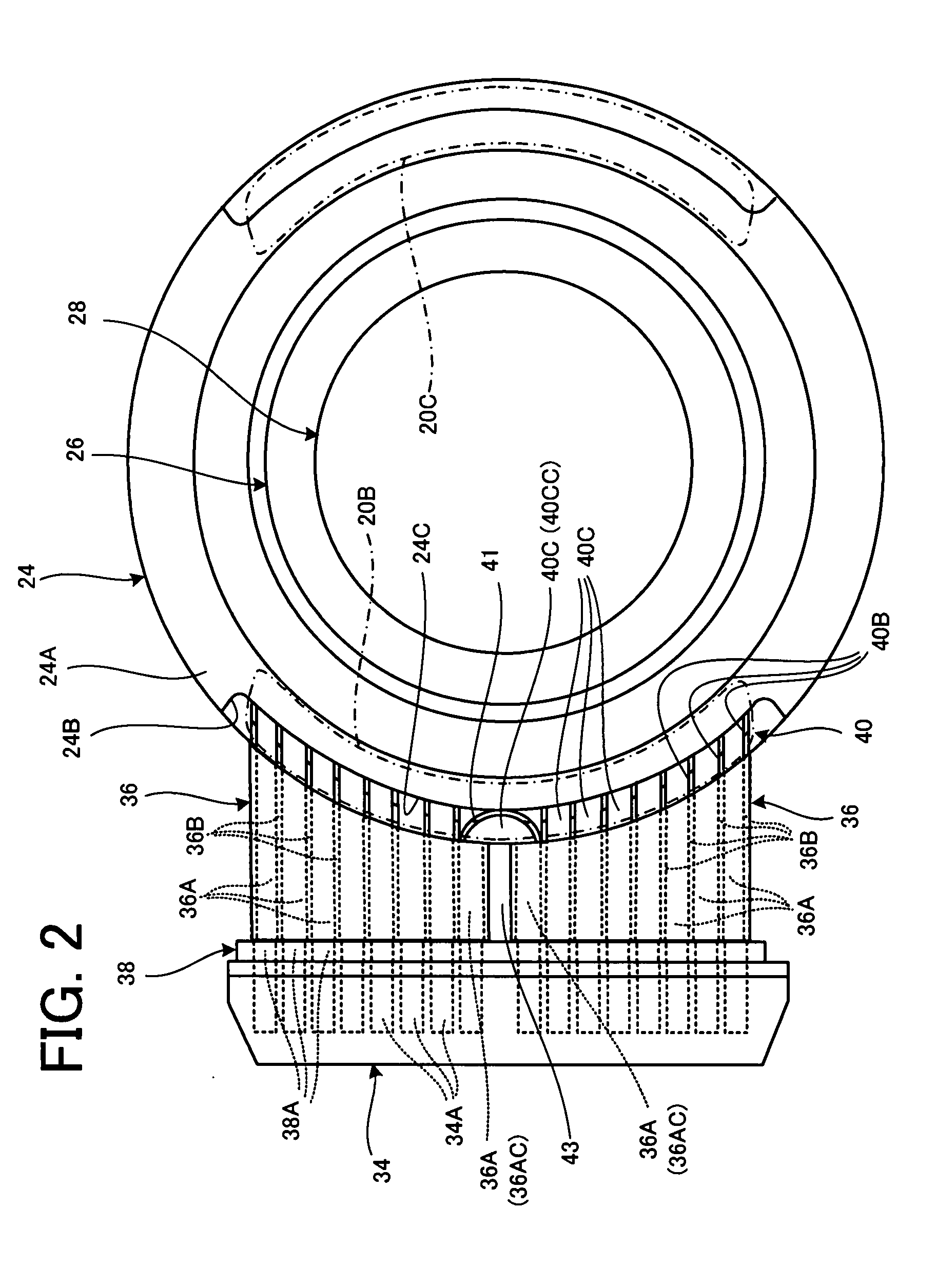
[0042]As shown in FIG. 1, the layer depositing reactor comprises an internal reaction device 20 having a reaction chamber 20A. The shape of the reaction chamber 20A is that of a substantially flat cylinder. The entire top surface of the reaction chamber 20A is covered by a substantially disc-shaped upper liner 22. In other words, the upper liner 22 forms the ceiling wall of the reaction chamber 20A. The bottom wall of the reaction device 20 is composed of a substantially circular lower liner 24 and a disc-shaped susceptor 26 disposed within a circul...


PUM

PropertyMeasurementUnit
Lengthaaaaaaaaaa
Lengthaaaaaaaaaa
Lengthaaaaaaaaaa

Abstract

A reactant gas is supplied to a gas inlet port 40B of a reaction chamber 20A from a plurality of gas flow paths 36A. The number of gas flow paths 36A is five or more within a range of one side of the gas inlet port 40B divided in two at the center thereof. The pitch between adjacent gas flow paths 36A is 10 mm or more. A baffle 38 having a plurality of slit holes 38A is disposed upstream of the gas flow paths 36A. The gas flow rates of the respective gas flow paths 36A are adjusted by recurrent calculation using layer growth sensitivity data that defines the relation between the gas flow rates of the respective gas flow paths 36A.

Description

CROSS-REFERENCE TO RELATED APPLICATIONS[0001]This application relates to and claims priority rights from Japanese Patent Application No. 2006-151356 and No. 2006-151374, both filed on May 31, 2006, the entire disclosures of which are hereby incorporated herein by reference.BACKGROUND OF THE INVENTION[0002]1. Field of the Invention[0003]The present invention relates to an apparatus and method for depositing a film or a layer such as an epitaxial layer on the surface of a substrate such as a semiconductor wafer.[0004]2. Description of the Related Art[0005]Japanese Patent No. 2641351 (JP-2641351-B) discloses a wafer processing reactor for vapor deposition of a silicon layer on the surface of a wafer. In such wafer processing reactor, an array of lamps is disposed at a top and a bottom of a reaction chamber, a rotating wafer pedestal is disposed horizontally at the center of the reaction chamber, and a gas inlet port and a gas exhaust port are provided on diametrically opposite sides of...

Claims


Application Information

Patent Timeline
IPC IPC(8): C23C16/00B05C11/00
CPCC23C16/52C23C16/45565
Inventor HIROSAWA, ATSUHIKOIIDA, NOBORUSATO, NORIHIKONAGATO, ATSUSHIKAMEI, TOSHIYUKINISHIKIDO, KOUICHINAKAMURA, MOTONORI
Owner SUMCO TECHXIV
Why Eureka
Try Eureka