Method of fabricating pmos thin film transistor

Inactive Publication Date: 2007-12-13
SAMSUNG MOBILE DISPLAY CO LTD
View PDF12 Cites 5 Cited by
  • Summary
  • Abstract
  • Description
  • Claims
  • Application Information

AI Technical Summary

Benefits of technology

[0010]Aspects of the present invention includes a method of fabricating a p-type thin film transistor (TFT), which includes crystallizing an amorphous silicon (a-Si) layer into a polycrystalline silicon (poly-Si) layer using a super grain silicon (SGS) method, patterning the crystallized layer, implanting gettering ion

Problems solved by technology

Nevertheless, the above methods have drawbacks in that the SPC method takes much time and needs a high-temperature annealing process to be performed for a long time so that the substrate is susceptible to deformation.
The ELC method not only requires an expensive laser apparatus, but also causes formation of polycrystalline protrusions, and deteriorates an interfacial characteristic between a semiconductor layer and a gate insulating layer.
In the MIC and MILC methods, a large amount of

Method used


Image

  • Method of fabricating pmos thin film transistor
  • Method of fabricating pmos thin film transistor
  • Method of fabricating pmos thin film transistor

Examples


Example

[0025]Reference will now be made in detail to the aspects of the present invention, examples of which are illustrated in the accompanying drawings, wherein like reference numerals refer to the like elements throughout. The aspects are described below in order to explain the present invention by referring to the figures.

[0026]It will be understood that when a layer is referred to as being “on” another layer or substrate, it can be directly on the other layer or substrate or intervening layers may also be present. In the drawings, the thicknesses of layers and regions are exaggerated for clarity.

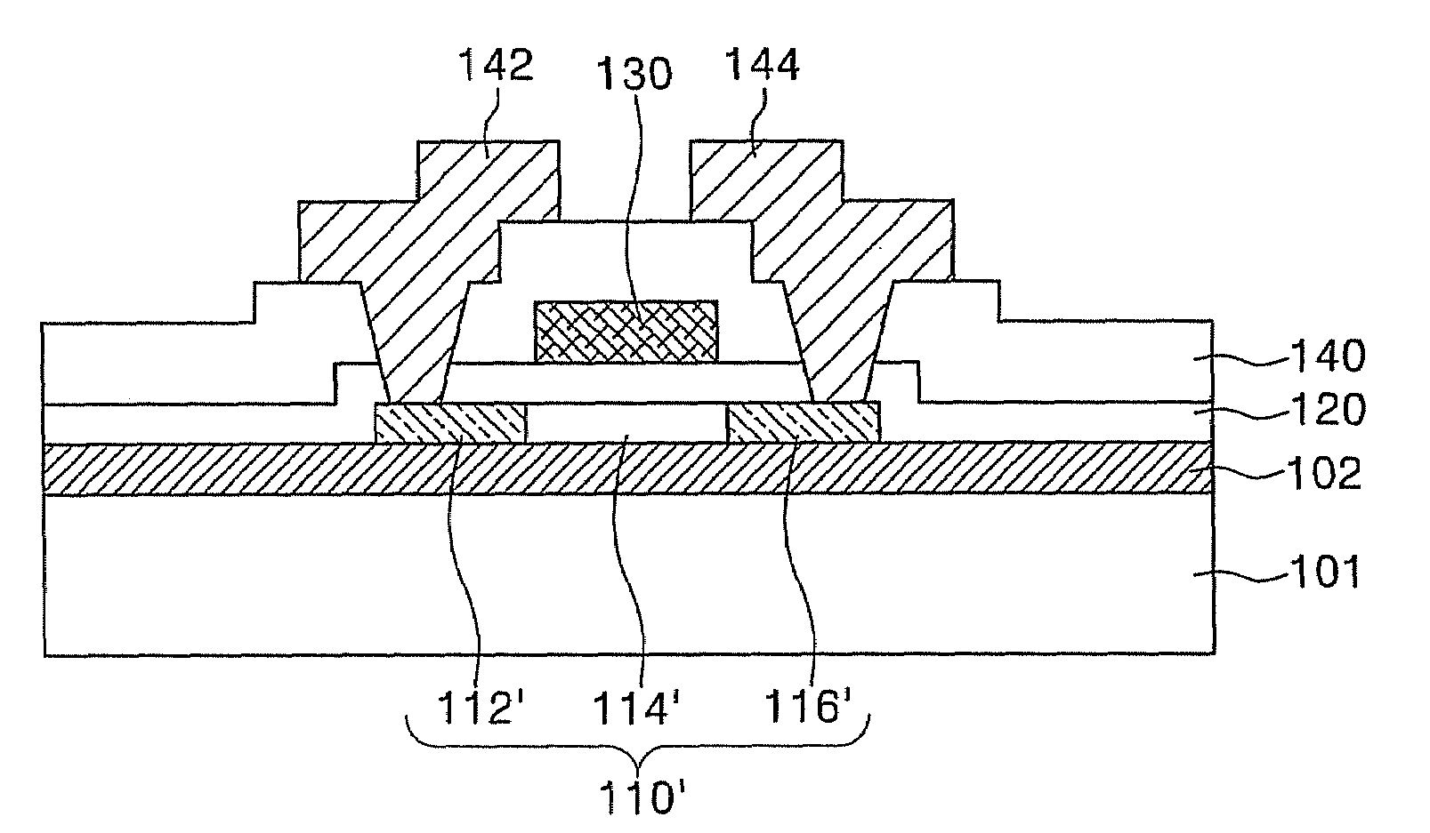
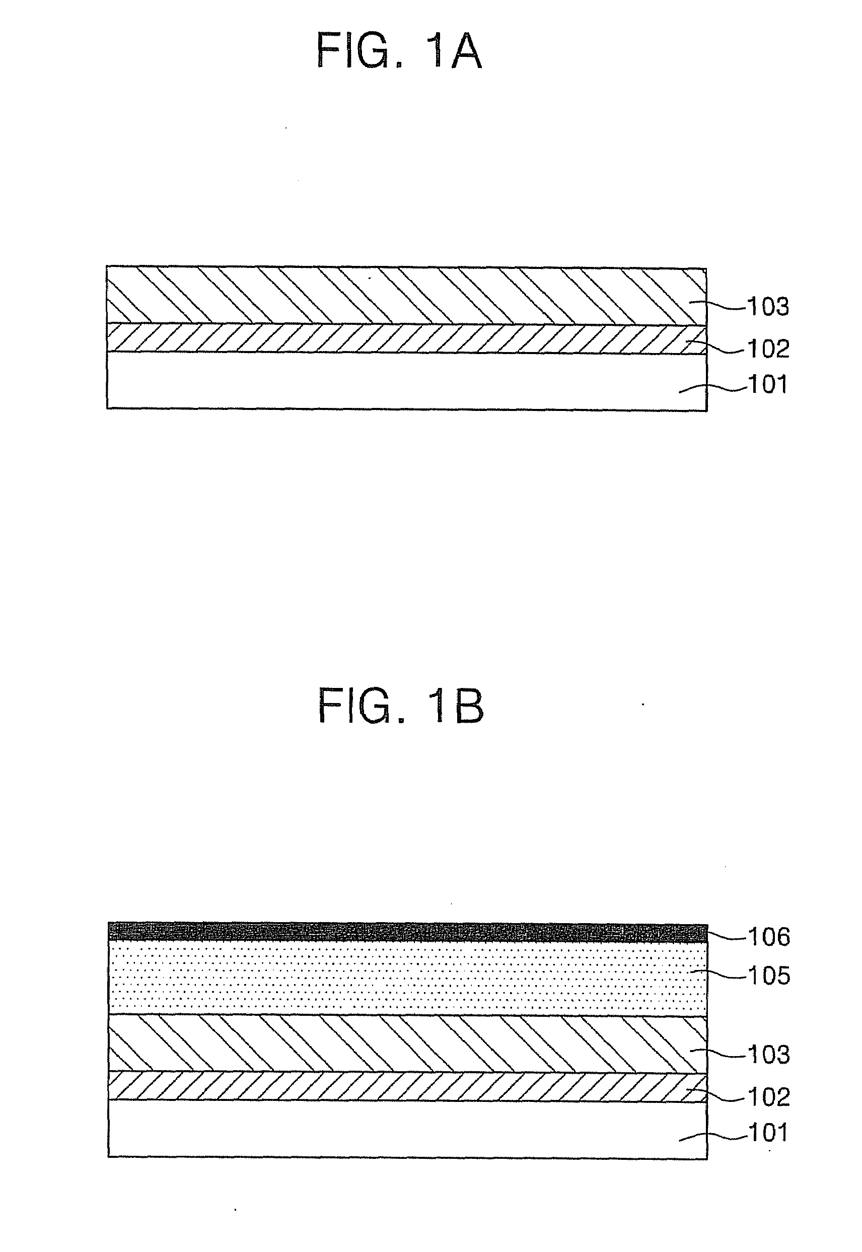
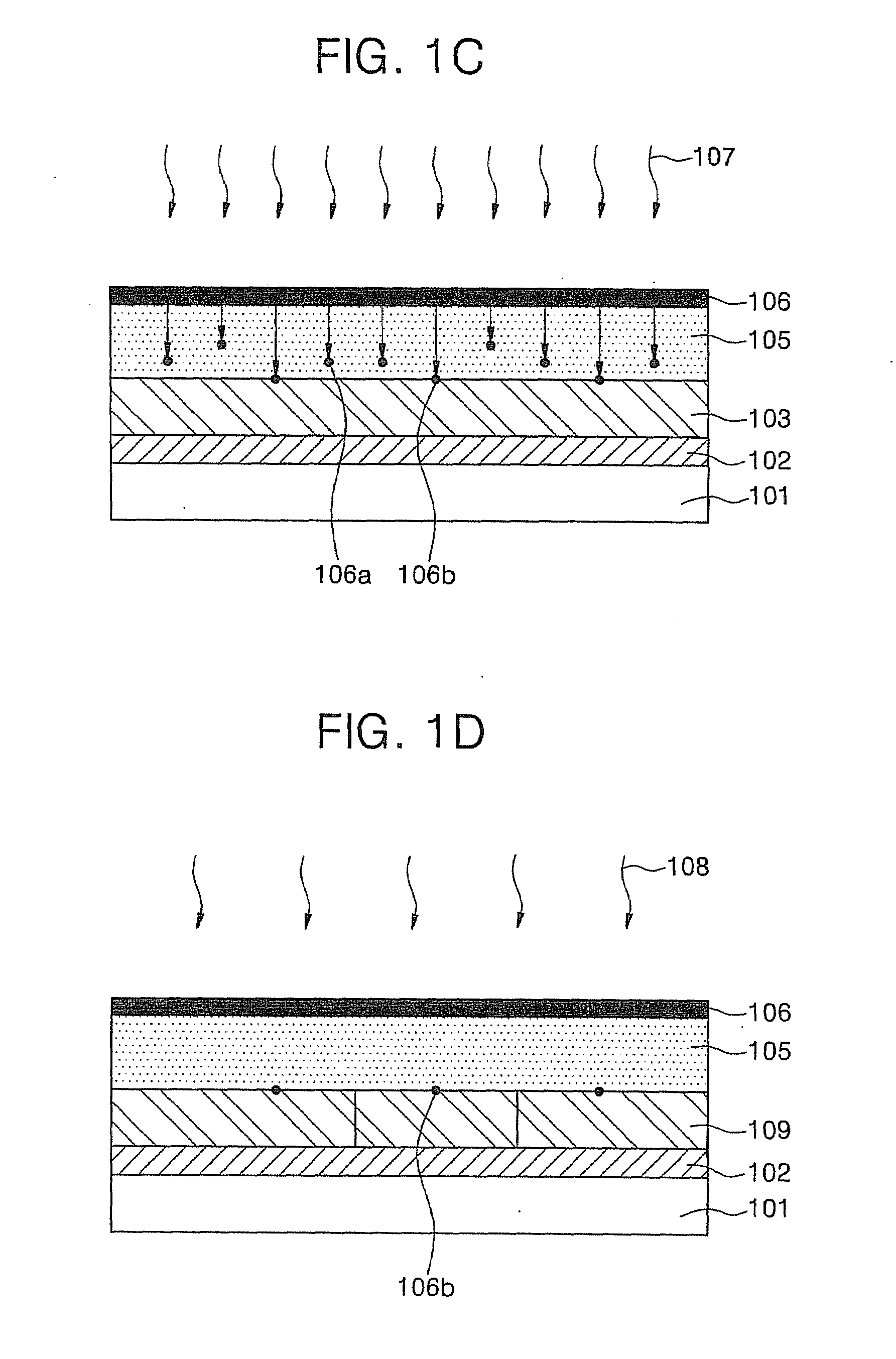
[0027]FIGS. 1A through 1D are cross-sectional views illustrating a crystallization process according to an aspect of the present invention. Referring to FIG. 1A, a buffer layer 102 is formed on a substrate 101 using a chemical vapor deposition (CVD) process or a physical vapor deposition (PVD) process. While not restricted thereto, the substrate 101 may be a glass substrate or a plastic substr...


PUM


Abstract

A method of fabricating a p-type thin film transistor (TFT) includes: performing a first annealing process on a substrate to diffuse a metal catalyst through a capping layer into a surface of an amorphous silicon layer, and to crystallize the amorphous silicon layer to a polycrystalline silicon layer due to the diffused metal catalyst; removing the capping layer; patterning the polycrystalline silicon layer to form a semiconductor layer; forming a gate insulating layer and a gate electrode on the substrate; implanting p-type impurity ions into the semiconductor layer; and implanting a gettering material into the semiconductor layer and performing a second annealing process to remove the metal catalyst. Herein, the p-type impurity ions are implanted at a dose of 6×10¹³/cm2 to 5×10¹⁵/cm2, and the gettering material is implanted at a dose of 1×10¹¹/cm2 to 3×10¹⁵/cm2.

Description

CROSS-REFERENCE TO RELATED APPLICATION[0001]This application claims the benefit of Korean Application No. 2006-44814, filed May 18, 2006 in the Korean Intellectual Property Office, the disclosure of which is incorporated herein by reference.BACKGROUND OF THE INVENTION[0002]1. Field of the Invention[0003]Aspects of the present invention relate to a method of fabricating a p-type thin film transistor (TFT). More particularly, aspects of the present invention relate to a method of fabricating a p-type TFT that includes crystallizing an amorphous silicon (a-Si) layer into a polycrystalline silicon (poly-Si) layer using a super grain silicon (SGS) method, patterning the crystallized layer, implanting gettering ions into source and drain regions of a semiconductor layer, and annealing the resultant structure to remove the very small amount of metal catalyst (e.g., Ni) that remains in the semiconductor layer. Accordingly, the amount of metal catalyst remaining in the semiconductor layer ca...

Claims


Application Information

Patent Timeline
IPC IPC(8): H01L21/335H01L29/04
CPCH01L21/02422H01L21/02488H01L27/1277H01L21/02672H01L29/66757H01L21/02532
Inventor YANG, TAE-HOONLEE, KI-YONGSEO, JIN-WOOKPARK, BYOUNG-KEON
Owner SAMSUNG MOBILE DISPLAY CO LTD
Why Eureka
Try Eureka