

Semiconductor device
a technology of semiconductor devices and semiconductors, applied in semiconductor devices, digital storage, instruments, etc., can solve the problems of increasing threshold voltage and writing current cannot be secured, and achieve the effect of stable reading operation
- Summary
- Abstract
- Description
- Claims
- Application Information
AI Technical Summary
Benefits of technology
Problems solved by technology
Method used
Image

Examples
embodiment 1
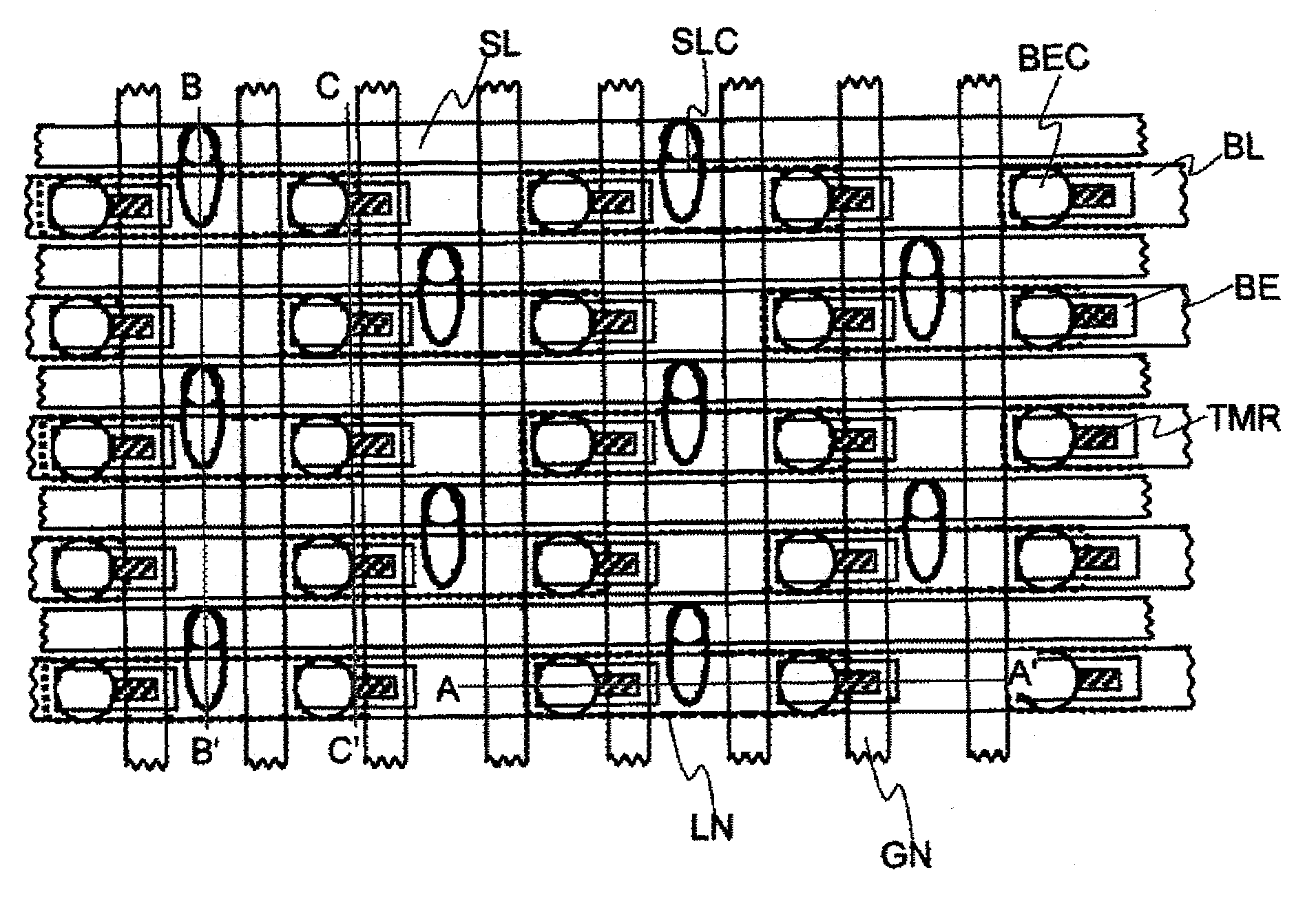
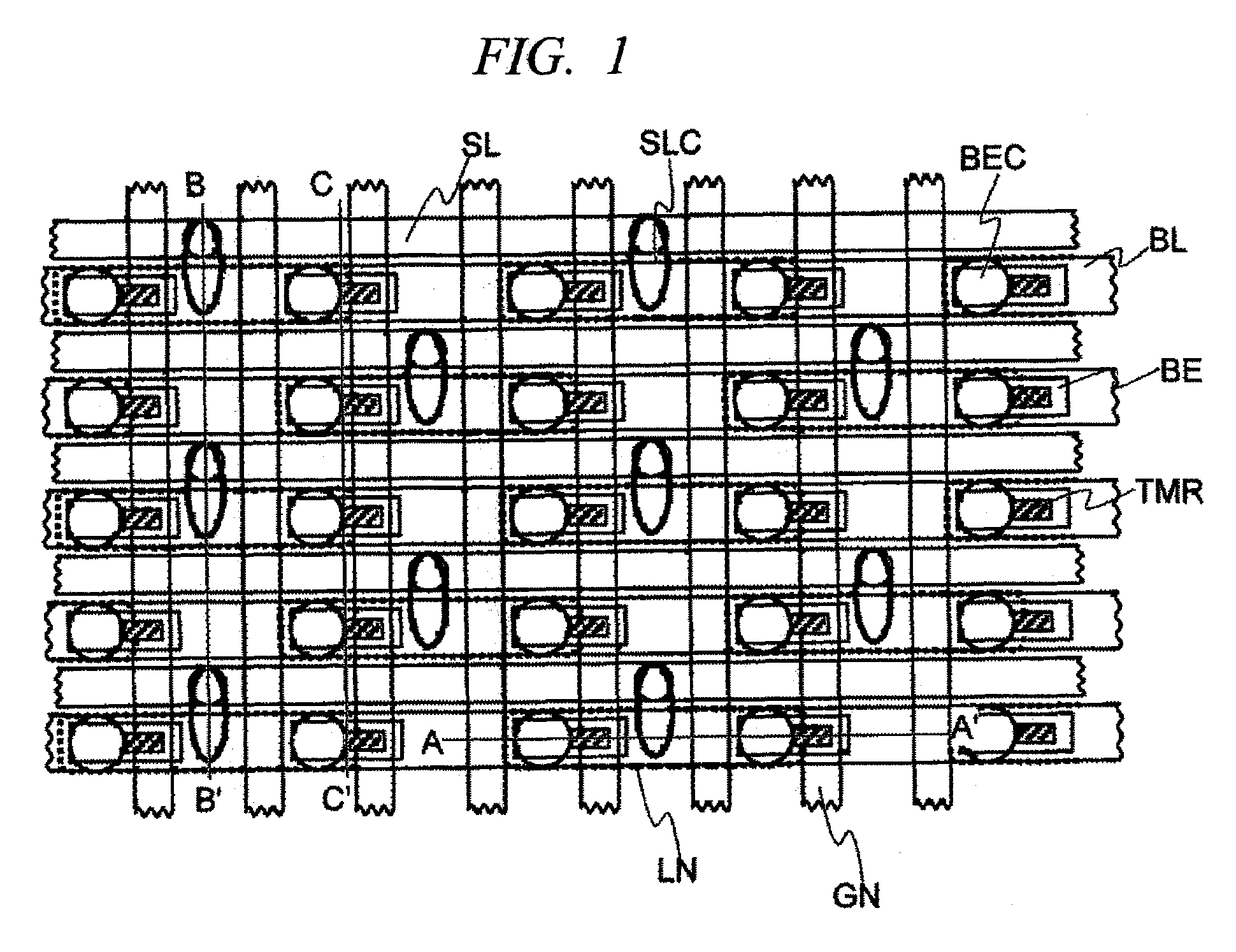
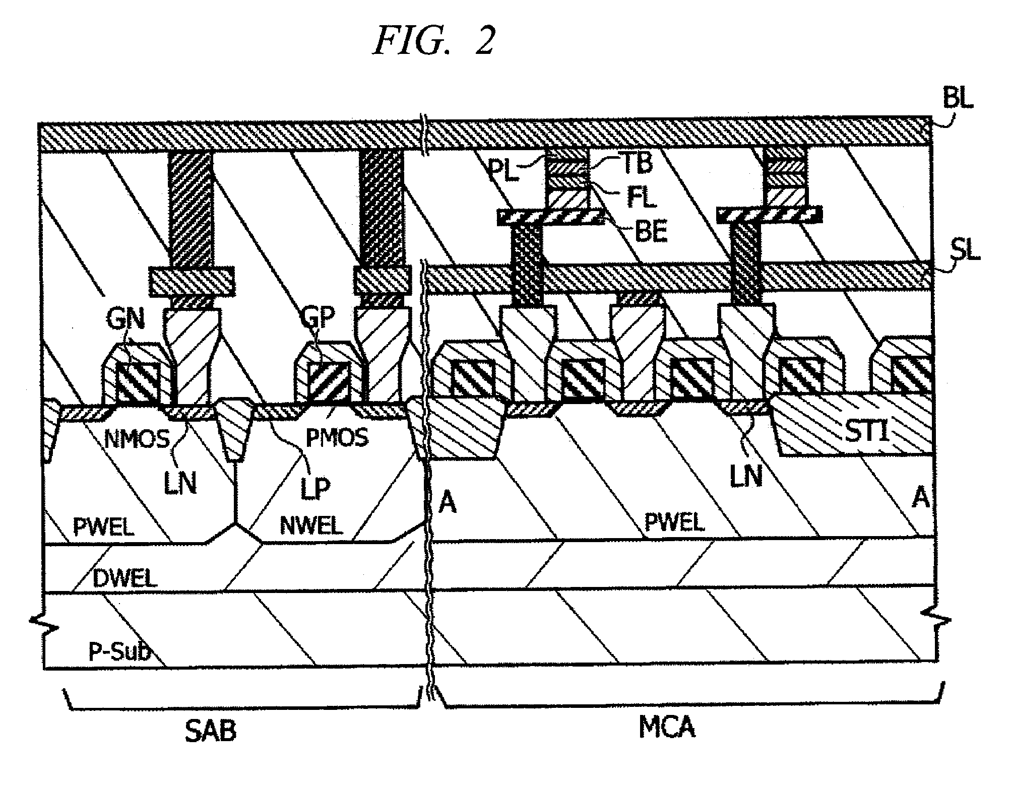
[0047]A first embodiment of the present invention will be explained. The present memory cell is composed of an N-type MOS transistor and a tunnel magneto-resistance element TMR. This structure is characterized in the arrangement of the free layer FL and the fixed layer PL of the tunnel magneto-resistance element TMR, in the case where the memory cell transistor MNT is the NMOS type, the free layer FL is arranged on the side of the transistor and the fixed layer PL is arranged on the side of the common wiring, in this case the bit lines BL. In this structure, the anti-parallel writing operation which requires a larger current compared with the parallel writing operation, can be performed by the source grounding in which the current driving power is large. Furthermore, in the reading operation a voltage is applied in the same direction as the anti-parallel writing direction to increase the reading current while preventing an error in writing. FIG. 1 is a layout view of a memory cell s...
embodiment 2
[0066]There will be explained the second embodiment of the present invention by reference to FIGS. 23 through 25. In this structure, on a lower portion of the tunnel magneto-resistance element TMR which constitutes a memory cell, writing bit lines WBL for exciting a magnetic field for reducing the writing current at the writing time are arranged. As a consequence, as compared with the current at the normal spin-transfer torque switching, the current which flows through the tunnel magneto-resistance element TMR can be reduced, so that the memory cell transistor can be made smaller in size and the drive voltage at the writing can be reduced. FIG. 23 is a layout example of a memory cell array according to the second embodiment. The area of the memory cell array is 8F2 at the minimum. In the second embodiment, the tunnel magneto-resistance element TMR is shifted and arranged in an extension direction of the word lines with respect to the bottom electrode contact. On the layer lower than...
PUM
 Abstract
Description
Claims
Application Information