

Semiconductor device
a technology of semiconductor devices and semiconductors, applied in the direction of semiconductor devices, basic electric elements, electrical equipment, etc., can solve the problems of poor process consistency of dram and logic transistors, and achieve the effect of stable reading operation
- Summary
- Abstract
- Description
- Claims
- Application Information
AI Technical Summary
Benefits of technology
Problems solved by technology
Method used
Image

Examples
first embodiment
[0107] (First Embodiment)
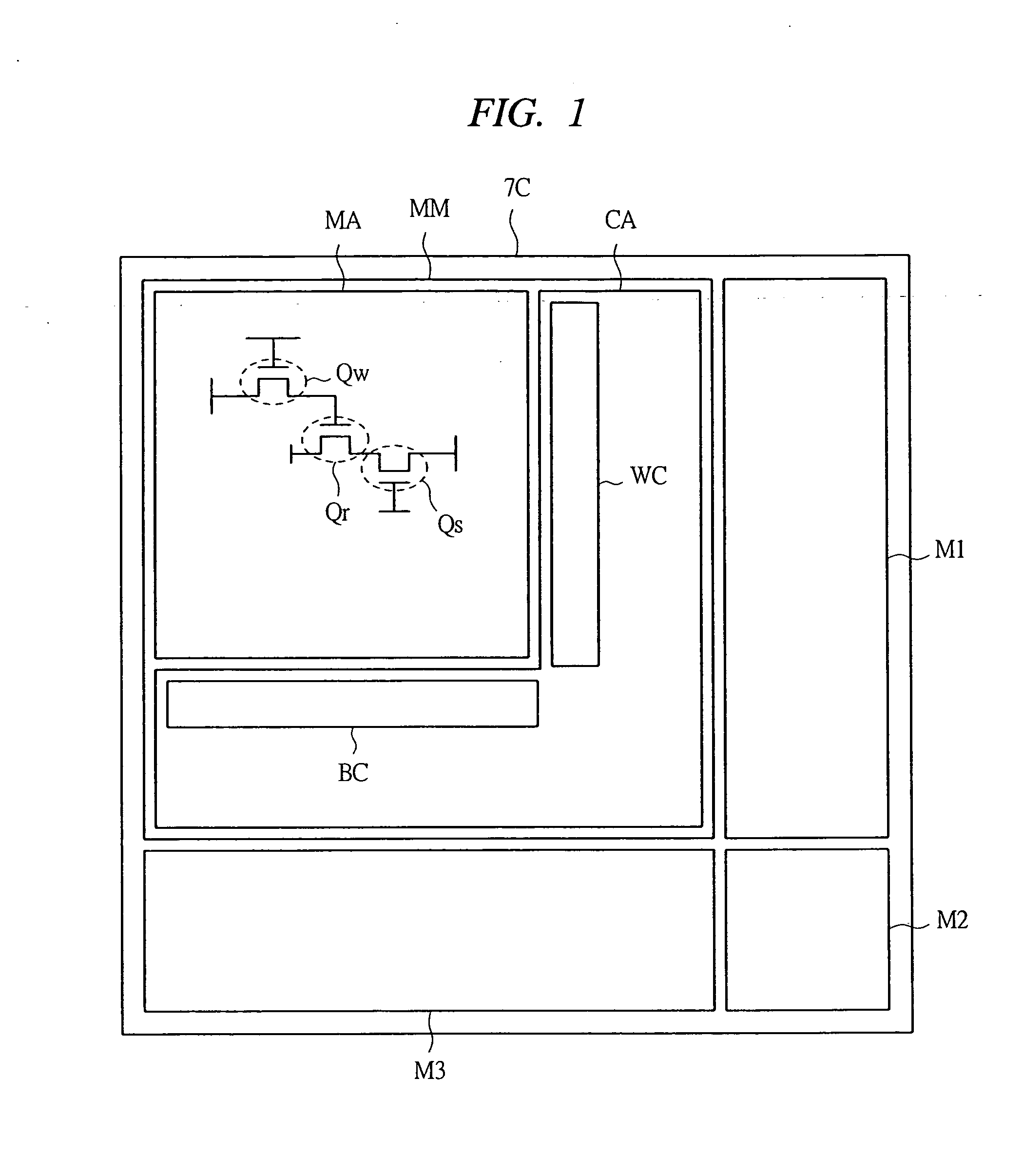
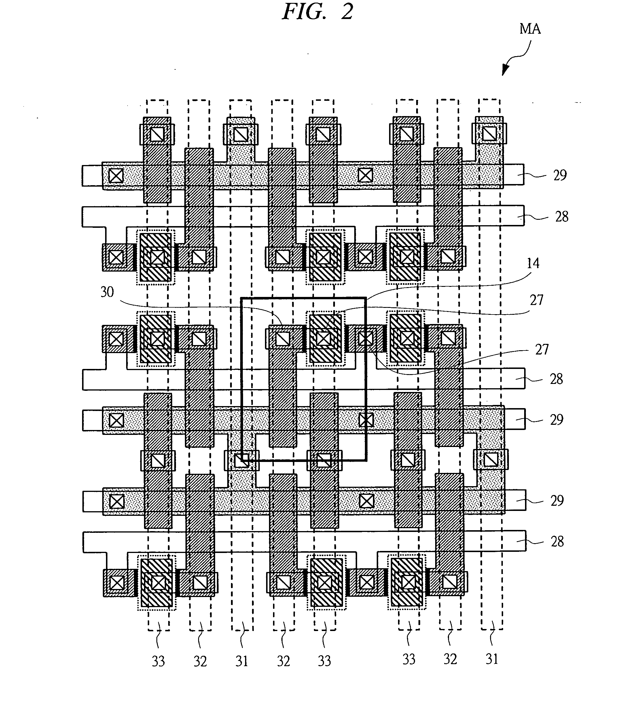
[0108]FIG. 1 is a schematic drawing for describing the structure of a semiconductor device according to a first embodiment of the present invention. For example, a semiconductor device in a chip (semiconductor chip) state has a chip 7C on which a memory module MM and modules M1, M2, and M3, such as other logic circuits (logic modules) and an analog circuit (analog module) are configured. In the memory module MM, a memory area MA and its peripheral circuit area CA are configured. In the memory area MA, a memory configured as an array of a plurality of memory cells is formed. Also, in the peripheral circuit area CA, a word line driving circuit WC and a bit line driving circuit BC for selecting a memory cell, and a peripheral circuit formed of a control circuit and others are formed.
[0109] A transistor forming these memory area MA and the peripheral circuit area CA is formed on one chip 7C. In the first embodiment, the memory area MA has a write transistor Qw,...
second embodiment
[0165] (Second Embodiment)
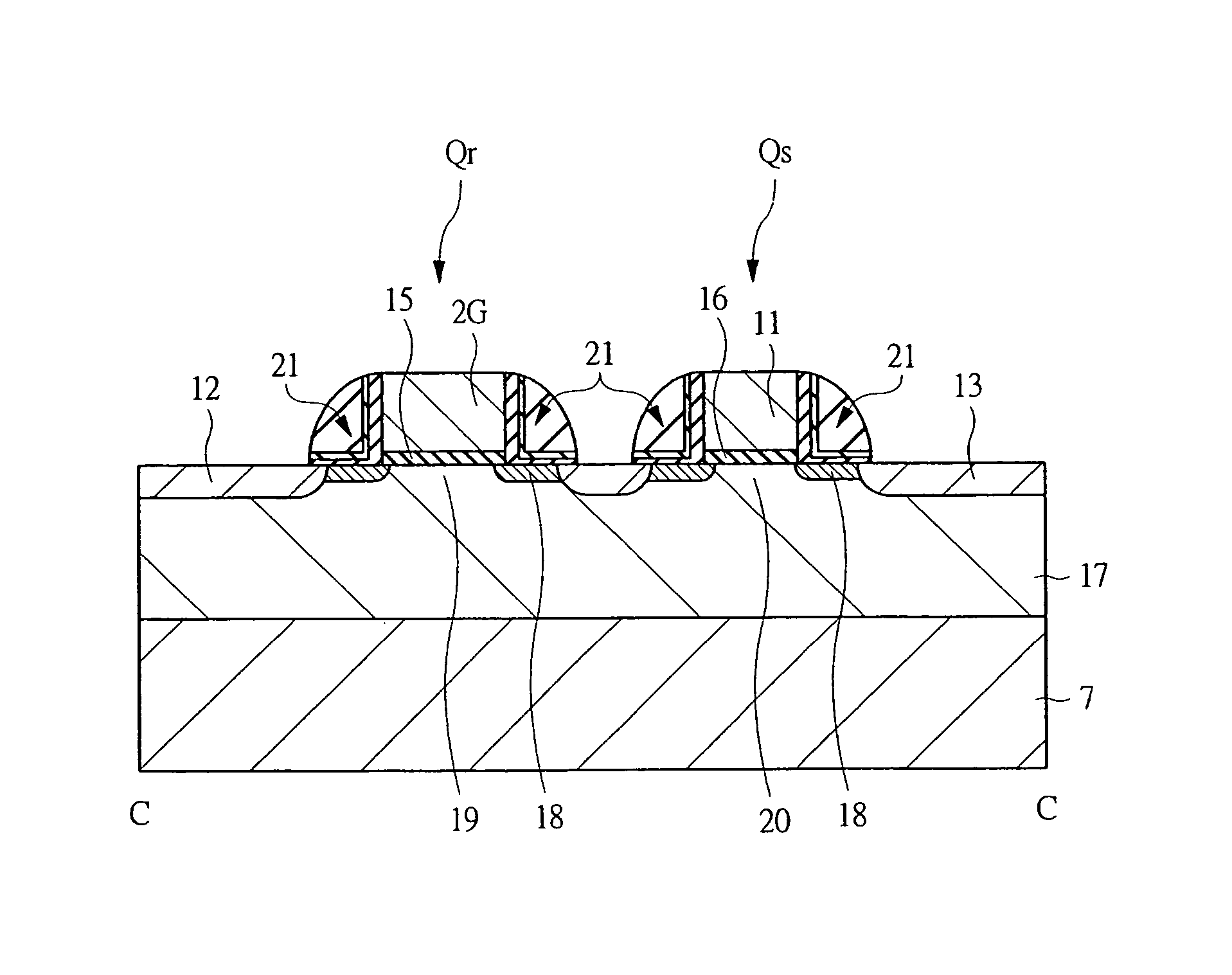
[0166] A semiconductor device according to a second embodiment is described with reference to FIGS. 24 to 28, focusing on differences from the first embodiment. FIG. 24 is a schematic plan view of a memory cell according to the second embodiment, depicting a write transistor Qw, a read transistor Qr, and a select transistor Qs. FIG. 25 is a cross-section view along an A-A line in FIG. 24. FIGS. 26 to 28 are schematic plan views of a memory cell during a manufacturing process in a region corresponding to FIG. 24.
[0167] First, the structure of the write transistor Qw of a unit memory cell according to the second embodiment is described. The structure of the write transistor Qw of FIG. 4 according to the first embodiment is such that the overlapped portion 8 of the gate on the upper surface of the source in the write transistor Qw of FIG. 71 studied by the inventors is eliminated. In the second embodiment, the structure does not include the facing portion 9. ...
third embodiment
[0178] (Third Embodiment)
[0179] A semiconductor device according to a third embodiment is described with reference to FIGS. 29 to 35, focusing on differences from the first embodiment. FIG. 29 is a schematic plan view of a memory cell according to the third embodiment, depicting a write transistor Qw, a read transistor Qr, and a select transistor Qs. FIG. 30 is a cross-section view along an A-A line in FIG. 29. FIG. 31 is a schematic plan view of the memory cell during a manufacturing process in a region corresponding to FIG. 29. FIGS. 32 to 35 are schematic cross-section views of the memory cell during the manufacturing process in a portion corresponding to the portion along the A-A line in FIG. 29. Here, in FIGS. 29 and 30, for ease of description of an element structure, components, such as contacts and wirings, are omitted. Also, in FIG. 29, an insulating film 36 shown in FIG. 30 is omitted for ease of viewing.
[0180] First, the structure of the write transistor Qw of a unit mem...
PUM
 Abstract
Description
Claims
Application Information