Semiconductor memory device

a memory device and semiconductor technology, applied in static storage, digital storage, instruments, etc., can solve the problems of large problems in the implementation of low-power semiconductor memory devices, impaired function of semiconductor memory devices, and increased production costs of semiconductor memory devices. , to achieve the effect of reducing substrate bias effect, increasing not only the size of semiconductor memory devices, and stable reading operation

Inactive Publication Date: 2006-07-20
SOCIONEXT INC
View PDF5 Cites 3 Cited by
  • Summary
  • Abstract
  • Description
  • Claims
  • Application Information

AI Technical Summary

Benefits of technology

[0049] As described above, according to the inventions, the bit lines and the read circuit are connected with each other without the use of the column decoder including the transistors shown in the explanation of the conventional art. As a result, a semiconductor memory device can be implemented in which a stable reading operation can be effected even with the low power supply voltage without the influence of a high threshold resulting from the substrate bias effect developed at the transistors constituting the column decoder.
[0050] Furthermore, unlike the methods for lowering only the threshold voltage of the some transistors during manufacturing and for reducing the substrate bias effect through the boost of the gate voltage of the some transistors, there is no need to provide special steps of lowering the threshold voltage and to provide a booster circuit having a large area used to boost the gate voltage, so that increases not only in the size of the semiconductor memory device but its production cost can be suppressed.

Problems solved by technology

Therefore, the function of the semiconductor memory device is impaired.
However, because of the suppression of power consumption increased by the OFF leakage current of transistors, it is difficult to lower the threshold voltage at the transistors; hence, this not only exists as a determinant of the range of the power supply voltage with which the semiconductor memory devices operate but brings about a big problem in the implementation of low-power semiconductor memory devices.
In addition, to boost the gate voltage, there is a necessity to provide a booster circuit having a relatively large area, which brings about increases in not only the size of semiconductor memory devices but their production cost.

Method used


Image

  • Semiconductor memory device
  • Semiconductor memory device
  • Semiconductor memory device

Examples


first embodiment

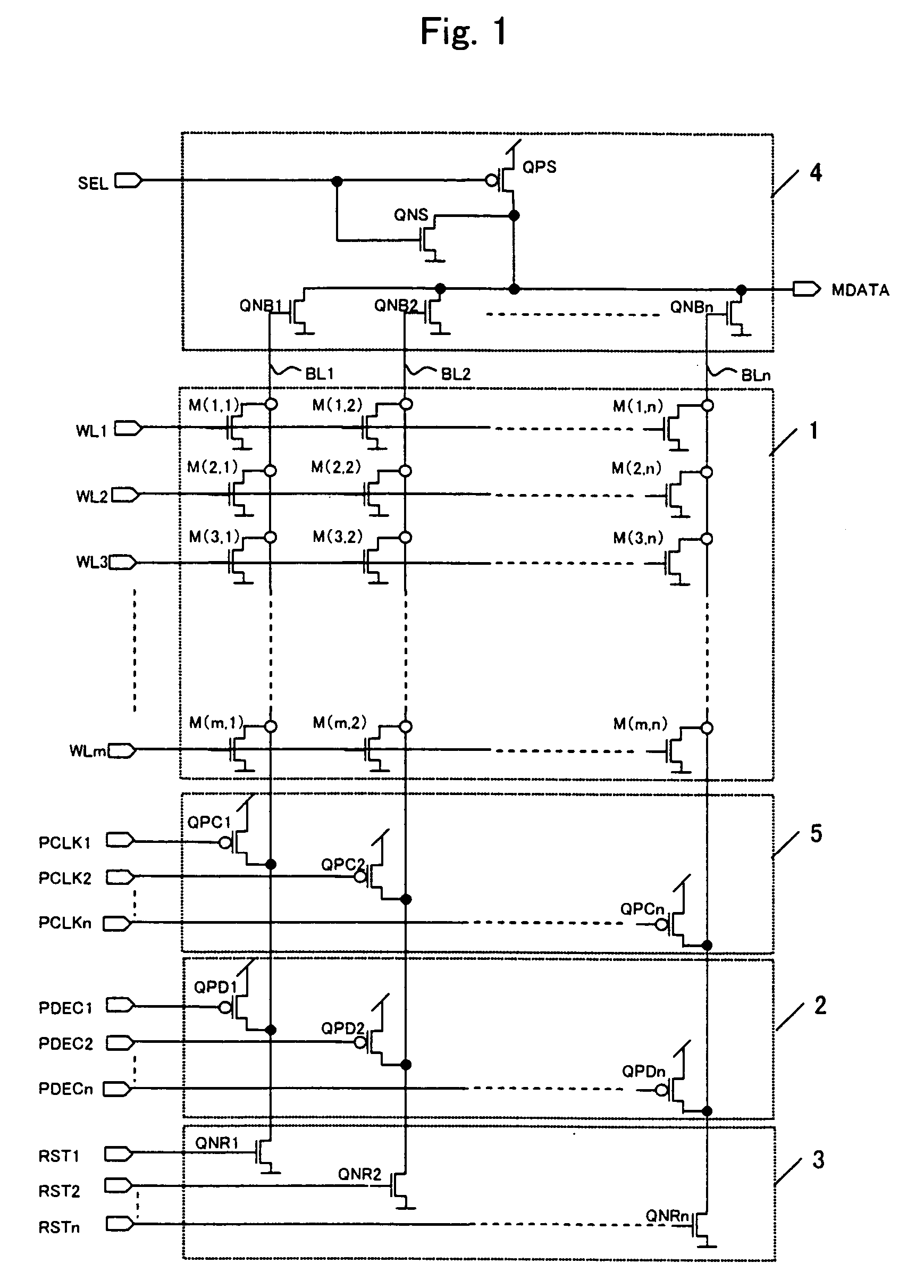
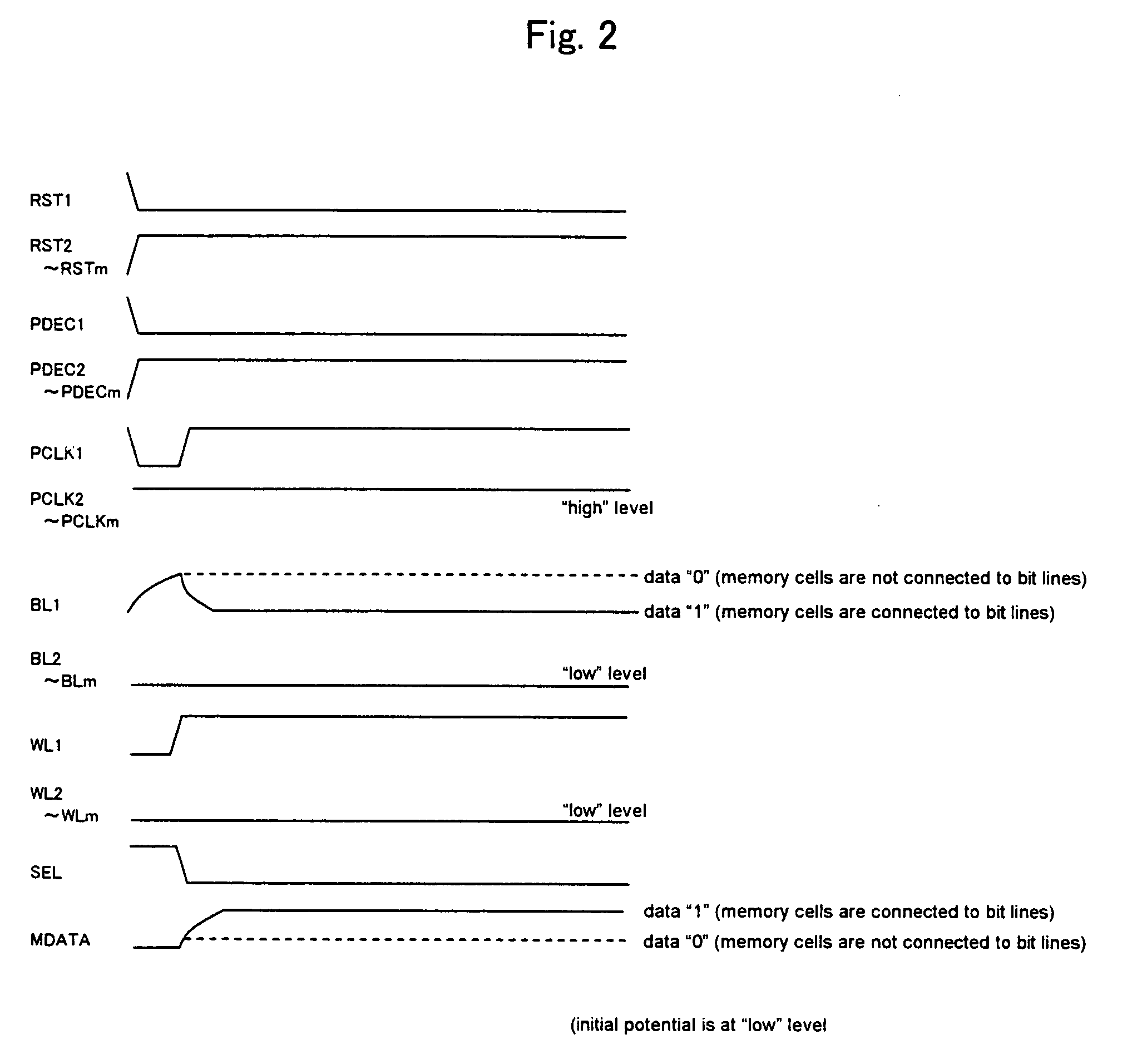
[0064]FIG. 1 is a circuit diagram showing the configuration of a semiconductor memory device according to a first embodiment of the present invention.

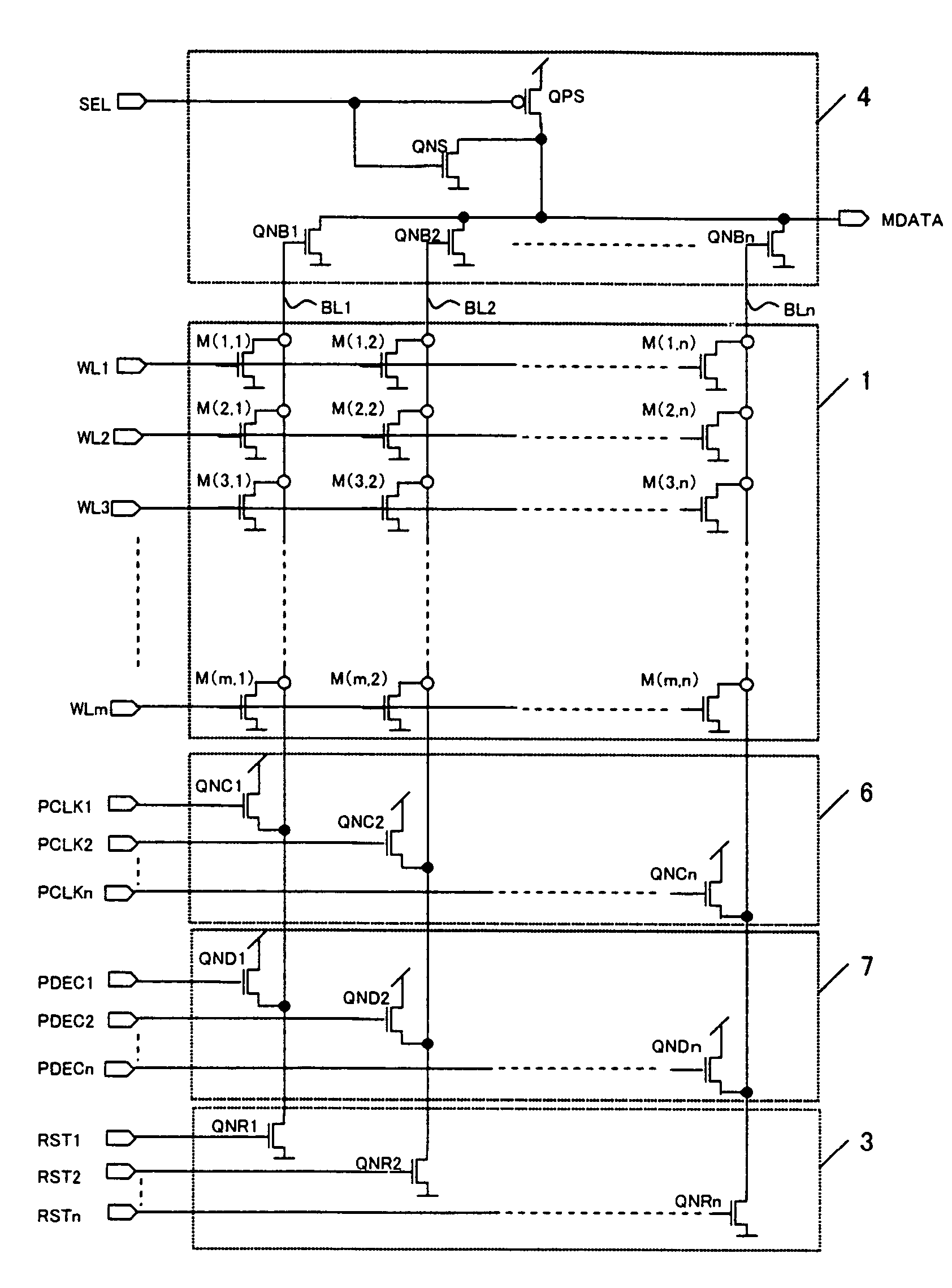
[0065] The semiconductor memory device shown in FIG. 1 includes a memory cell array 1, a bit line charge circuit 2, a bit line reset circuit 3, a read circuit 4, and a bit line precharge circuit 5.

[0066] Since the memory cell array 1 is the same as that of the conventional art semiconductor memory device, the explanation of the same components will be omitted instead of giving the same reference numerals.

[0067] The bit line charge circuit 2 includes P-type MOS transistors QPDj (j=1 to n). With the P-type MOS transistors QPDj (j=1 to n), their gates are each connected to charge selection signal lines PDECj (j=1 to n), their sources are connected to power supply potential lines, and their drains are each connected to bit lines BLj (j=1 to n).

[0068] The ON-state currents of the P-type MOS transistors QPDj (j=1 to n) are set so as to b...

second embodiment

[0088]FIG. 3 is a circuit diagram showing the configuration of a semiconductor memory device according to a second embodiment of the invention.

[0089] The semiconductor memory device shown in FIG. 3 includes the memory cell array 1, the bit line reset circuit 3, the read circuit 4, a bit line precharge circuit 6, and a bit line charge circuit 7. Since the memory cell array 1, the bit line reset circuit 3, and the read circuit 4 are the same as those described in the first embodiment, the explanation of the same components thereof will be omitted instead of giving the same reference numerals.

[0090] The bit line precharge circuit 6 includes N-type MOS transistors QNCj (j=1 to n). As for the N-type MOS transistors QNCj (j=1 to n), their gates are each connected to precharge selection signal lines PCLKj (j=1 to n), their drains are connected to power supply potential lines, and their sources are each connected to bit lines BLj (j=1 to n).

[0091] The bit line charge circuit 7 includes N...

third embodiment

[0107]FIGS. 5 and 6 are circuit diagrams showing the configuration of a semiconductor memory device according to a third embodiment of the invention.

[0108] As shown in FIG. 6, the semiconductor memory device according to the fourth embodiment includes a memory block 10, a memory block 11, and an output selection circuit 12.

[0109] As shown in FIG. 5, the memory blocks 10 and 11 are each constituted by the memory cell array 1, the bit line reset circuit 3, the read circuit 4, a bit line precharge circuit 8, and a bit line charge circuit 9. Since the memory cell array 1, the bit line reset circuit 3, and the read circuit 4 are the same as those described in the first embodiment, the explanation of the same components thereof will be omitted instead of giving the same reference numerals.

[0110] The bit line precharge circuit 8 includes P-type MOS transistors QPUj (j=1 to n) and N-type MOS transistors QNUj (j=1 to n).

[0111] As for the P-type MOS transistors QPUj (j=1 to n), their gate...


PUM


Abstract

A semiconductor memory device includes a memory cell array, a charge circuit which compensates for OFF leakage current developed at selected bit lines, a reset circuit having a ground potential corresponding to a potential at non-selected bit lines, a read circuit constituted by a plurality of transistors whose gates are connected to the bit lines, and a bit line precharge circuit which charges the selected bit lines for a fixed time period. As a result of adopting such a configuration, there is no need to provide a transmission gate, such as a column decoder, to a charging path between the read circuit and the bit lines, so that a low-power supply voltage operation can be effected without the influence of a substrate bias effect.

Description

BACKGROUND OF THE INVENTION [0001] 1. Field of the Invention [0002] The present invention relates to a semiconductor memory device and to a circuit technology through which a low-voltage operation is implemented. [0003] 2. Background Art [0004] Conventional art semiconductor memory devices include, for example, a semiconductor memory device disclosed in Patent Document 1, the configuration of a contact-type mask ROM is disclosed. [0005]FIG. 12 is a circuit diagram showing the configuration of the contact-type mask ROM. With the contact-type mask ROM, whether the drains of memory cell transistors are connected to bit lines corresponds to the “1” and “0” states of storage data. [0006] The conventional art semiconductor memory device shown in FIG. 12 includes a memory cell array 1, a column decoder 15, and a read circuit 16. [0007] The memory cell array 1 includes memory cells M(i, j) (i=1 to m, and j=1 to n) each composed of a N-type MOS transistor and arranged in matrix form. As for ...

Claims


Application Information

Patent Timeline
Patent Type & Authority Applications(United States)
IPC IPC(8): G11C7/00
CPCG11C7/12G11C17/12
Inventor HAYASHI, MITSUAKIABE, WATARUNAKAYA, SHUJIKURATA, MASAKAZU
Owner SOCIONEXT INC
Why Eureka
Try Eureka