
Semiconductor device

a technology of semiconductors and semiconductors, applied in the direction of semiconductor devices, electrical equipment, transistors, etc., can solve the problems of poor process consistency of dram and logic transistors, and achieve the effect of stable reading operation

Inactive Publication Date: 2012-01-31
RENESAS ELECTRONICS CORP
View PDF43 Cites 4 Cited by
  • Summary
  • Abstract
  • Description
  • Claims
  • Application Information

AI Technical Summary

Benefits of technology

The patent describes a DRAM memory cell with a gain-cell structure that uses a field-effect transistor with a small leakage current to achieve a long information retention time and a small power consumption. However, the small charge-storage capacitance of the memory cell can be significantly influenced by parasitic capacitance, which can lead to a decrease in information retention time. The technical effect of the patent is to provide a solution to reduce the impact of parasitic capacitance on the information retention time of the memory cell.

Problems solved by technology

Such DRAM has poor process consistency with logic transistors which form peripheral circuits of memory and other logical circuits.

Method used


Image

  • Semiconductor device
  • Semiconductor device
  • Semiconductor device

Examples


first embodiment

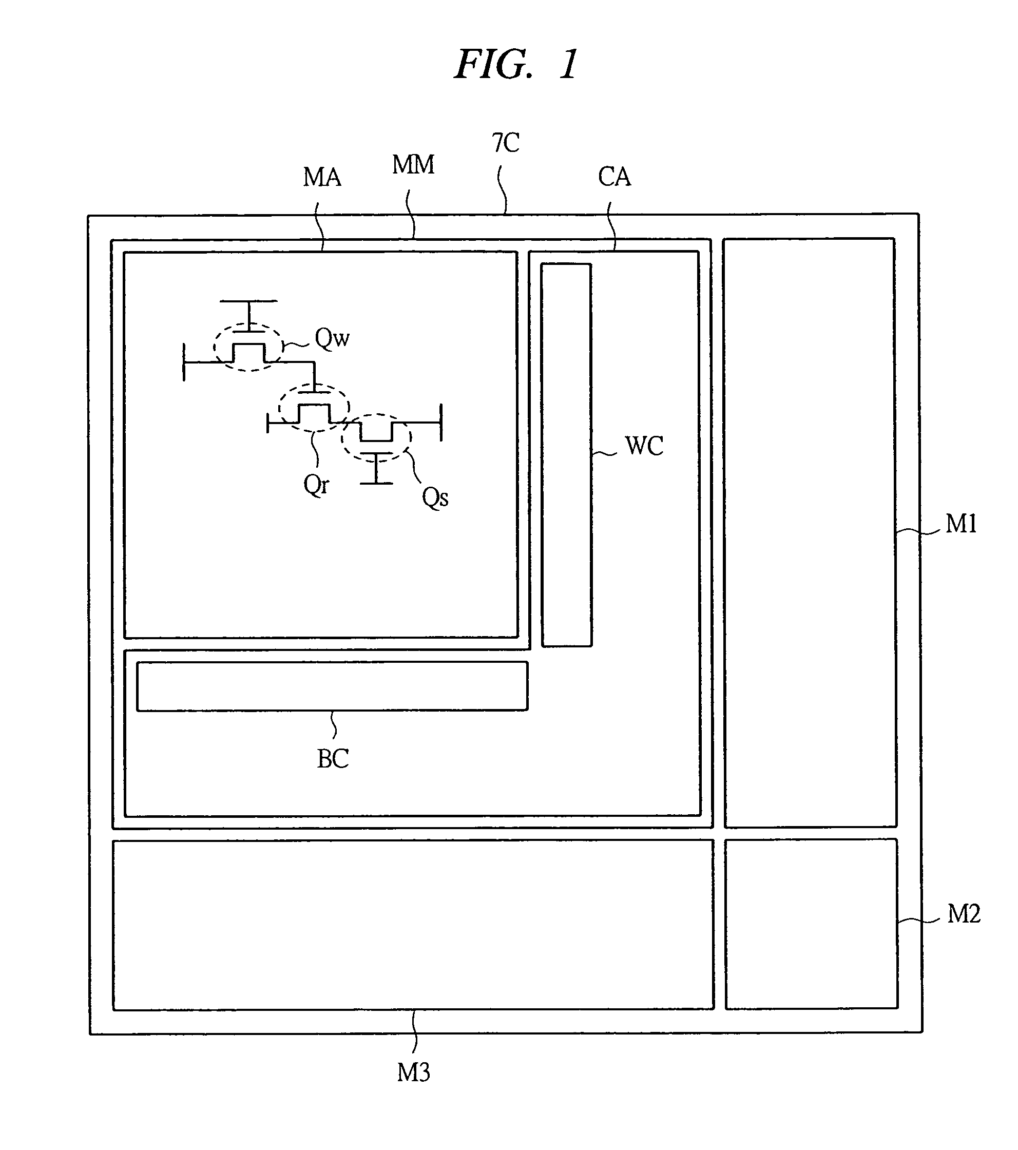
[0107]FIG. 1 is a schematic drawing for describing the structure of a semiconductor device according to a first embodiment of the present invention. For example, a semiconductor device in a chip (semiconductor chip) state has a chip 7C on which a memory module MM and modules M1, M2, and M3, such as other logic circuits (logic modules) and an analog circuit (analog module) are configured. In the memory module MM, a memory area MA and its peripheral circuit area CA are configured. In the memory area MA, a memory configured as an array of a plurality of memory cells is formed. Also, in the peripheral circuit area CA, a word line driving circuit WC and a bit line driving circuit BC for selecting a memory cell, and a peripheral circuit formed of a control circuit and others are formed.

[0108]A transistor forming these memory area MA and the peripheral circuit area CA is formed on one chip 7C. In the first embodiment, the memory area MA has a write transistor Qw, which is a transistor that...

second embodiment

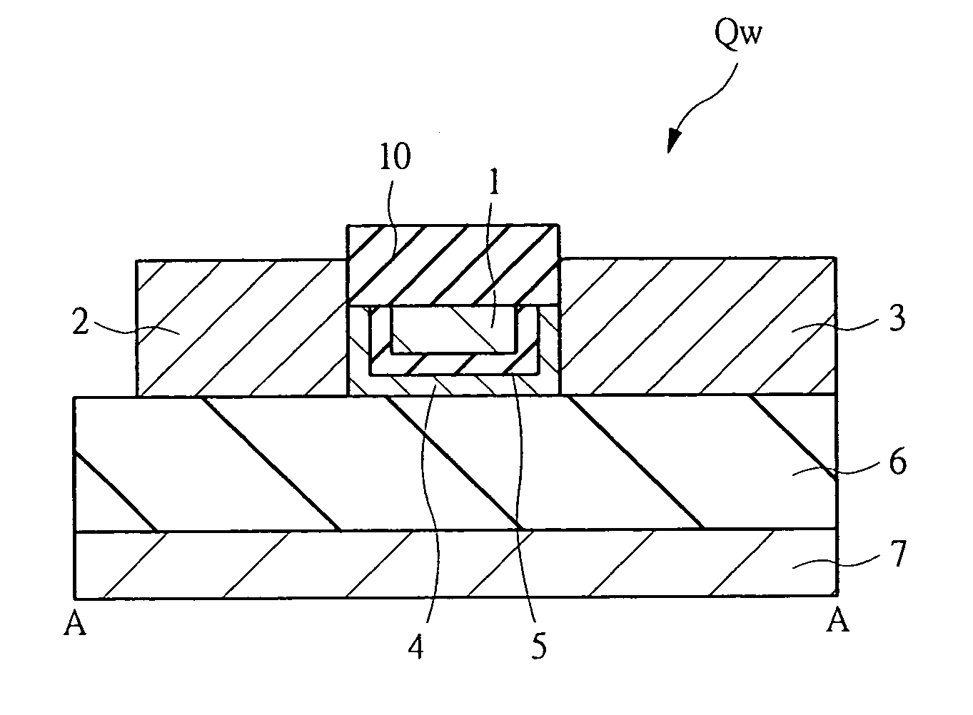
[0164]A semiconductor device according to a second embodiment is described with reference to FIGS. 24 to 28, focusing on differences from the first embodiment. FIG. 24 is a schematic plan view of a memory cell according to the second embodiment, depicting a write transistor Qw, a read transistor Qr, and a select transistor Qs. FIG. 25 is a cross-section view along an A-A line in FIG. 24. FIGS. 26 to 28 are schematic plan views of a memory cell during a manufacturing process in a region corresponding to FIG. 24.

[0165]First, the structure of the write transistor Qw of a unit memory cell according to the second embodiment is described. The structure of the write transistor Qw of FIG. 4 according to the first embodiment is such that the overlapped portion 8 of the gate on the upper surface of the source in the write transistor Qw of FIG. 71 studied by the inventors is eliminated. In the second embodiment, the structure does not include the facing portion 9. That is, as shown in FIGS. 24...

third embodiment

[0176]A semiconductor device according to a third embodiment is described with reference to FIGS. 29 to 35, focusing on differences from the first embodiment. FIG. 29 is a schematic plan view of a memory cell according to the third embodiment, depicting a write transistor Qw, a read transistor Qr, and a select transistor Qs. FIG. 30 is a cross-section view along an A-A line in FIG. 29. FIG. 31 is a schematic plan view of the memory cell during a manufacturing process in a region corresponding to FIG. 29. FIGS. 32 to 35 are schematic cross-section views of the memory cell during the manufacturing process in a portion corresponding to the portion along the A-A line in FIG. 29. Here, in FIGS. 29 and 30, for ease of description of an element structure, components, such as contacts and wirings, are omitted. Also, in FIG. 29, an insulating film 36 shown in FIG. 30 is omitted for ease of viewing.

[0177]First, the structure of the write transistor Qw of a unit memory cell according to the th...


PUM

PropertyMeasurementUnit
thicknessaaaaaaaaaa
thicknessaaaaaaaaaa
thicknessaaaaaaaaaa

Abstract

To achieve a stable reading operation in a memory cell having a gain-cell structure, a write transistor is configured, which has a source and a drain that are formed on the insulating layer, a channel formed on the insulating layer and between the source and the drain and made of a semiconductor, and a gate formed on an upper portion of the insulating layer and between the source and the drain and electrically insulated from the channel by a gate insulating film and controlling the potential of the channel. The channel electrically connects the source and the drain on the side surfaces of the source and the drain.

Description

CROSS-REFERENCE TO RELATED APPLICATION[0001]The present application claims priority from Japanese Patent Application No. JP 2005-270816 filed on Sep. 16, 2005, the content of which is hereby incorporated by reference into this application.TECHNICAL FIELD OF THE INVENTION[0002]The present invention relates to semiconductor devices and, particularly, to a technology effective when applied to a semiconductor device including a memory cell having a gain-cell structure.BACKGROUND OF THE INVENTION[0003]As microfabrication progresses, many transistors have become able to be integrated on the same chip, and also circuits with many functions have become able to be mounted on the same chip. On-chip memory having a memory and a processor mixed on the same chip is superior in both of data transfer rate and power consumption, compared with the case where memory is separately mounted on another chip. In particular, as mobile devices including cellular phone and PDA (Personal Digital Assistance) b...

Claims


Application Information

Patent Timeline
Patent Type & Authority Patents(United States)
IPC IPC(8): H01L29/94
CPCH01L27/11H01L27/115H01L29/78H01L27/1203H01L29/41783H01L27/11517H10B10/00H10B41/00H10B69/00
Inventor SANO, TOSHIAKIISHII, TOMOYUKIKAMESHIRO, NORIFUMIMINE, TOSHIYUKI
Owner RENESAS ELECTRONICS CORP
Learn More