Fabrication of full-color OLED panel using micro-cavity structure

Inactive Publication Date: 2007-12-13
ITC LIMITED
View PDF5 Cites 120 Cited by
  • Summary
  • Abstract
  • Description
  • Claims
  • Application Information

AI Technical Summary

Problems solved by technology

One problem is that the different efficiency of the 3 device of RGB will need different design of the driving circuit.
The other problem is that the different lifetime will conduce unequal of the color that will be compensated with the circuit but then increase the difficul

Method used


Image

  • Fabrication of full-color OLED panel using micro-cavity structure
  • Fabrication of full-color OLED panel using micro-cavity structure
  • Fabrication of full-color OLED panel using micro-cavity structure

Examples


example 1

Using White Organic Electroluminescence on Emission Layer 6

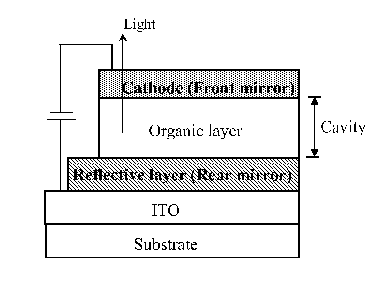
[0050]The example uses the bottom-emitting WRGB full-color OLED shown in FIG. 4. The hole injection layer 4 is m-MTDATA:F4-TCNQ (3%), and the thickness of white, blue, green and red light devices is 55 nm, 55 nm, 75 nm, and 105 nm, respectively. The structure of the emission layer 6 is NPB (15 nm) / NPB:Rubrene (5 nm) / DPVBi:BCzVBi (15 nm) / DPVBi:DCJTB (1 nm), and the electron transport layer 7 is Alq3 (20 nm). The total-reflective metal cathode 8 is LiF (0.7 nm) / Al (180 nm), and the semi-reflective metal anode 3 is Ag (50 nm). The Ag membrane on the ITO electrode 2 of the blue, green, and red light OLEDs must be processed with 100 watt O2 plasma for 30 to 180 seconds to increase the work function of Ag to enhance the efficiency of hole injection.

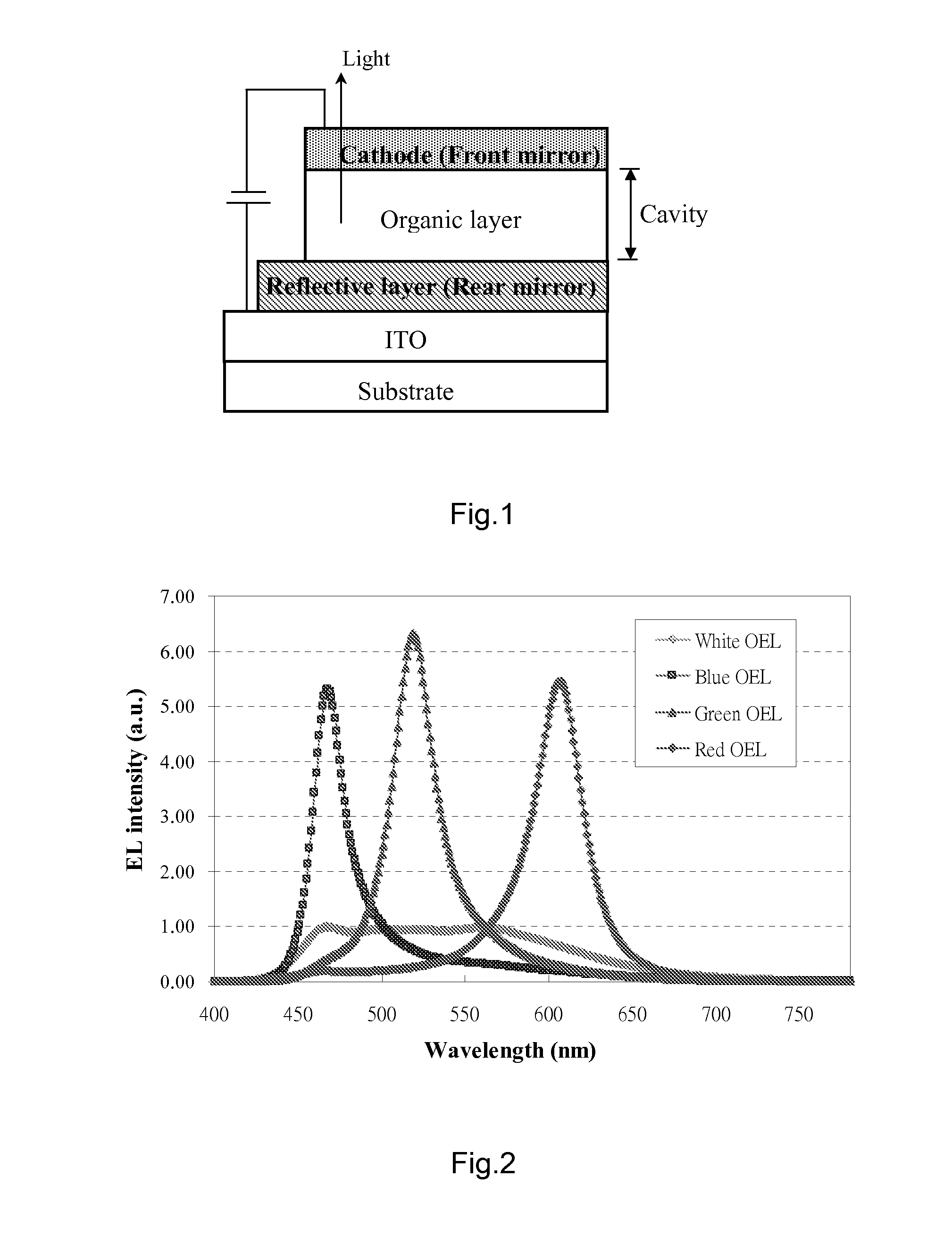
[0051]FIGS. 8 & 9 show the actual measured values and simulated values of electroluminescence spectrum and CIE chromaticity coordinates of white OLED under circuit of 50 mA / cm2, and blu...

example 2

Using Green Organic Electroluminescence on Emission Layer 6

[0054]On the other hand, the emission layer 6 in our invention also can use the green organic electroluminescence. We take the full-color bottom-emitting OLED in FIG. 5 as an example. The composition of the hole injection layer 4 is m-MTDATA:F4-TCNQ (3%) (x nm), and the thickness (x) for blue, green, and red light are 70 nm, 85 nm, and 115 nm, respectively. The structure of the emission layer 6 is NPB (20 nm) / Alq3 (20 nm), and the electron transport layer 7 is Alq3 (20 nm). The total reflective metal cathode 8 is LiF (0.7 nm) / Al (180 nm), and the semi-reflective metal anode 3 is Ag (50 nm). The Ag membrane on ITO 2 of the blue, green, and red light OLEDs must be processed with 100 watt O2 plasma for 30 to 180 seconds to increase the work function of Ag to elevate the efficiency of hole injection.

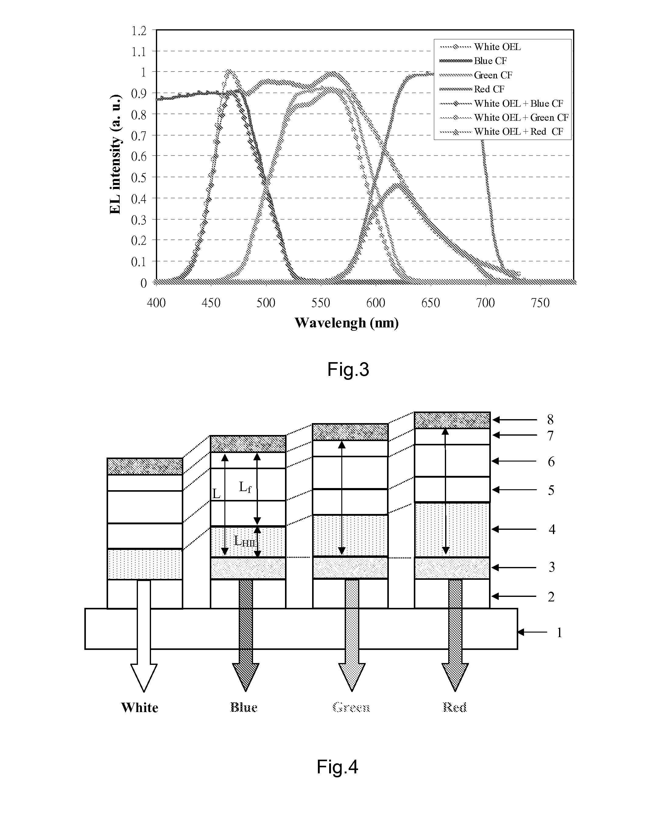
[0055]FIGS. 12 & 13 show the actual measured values and simulated values of electroluminescence spectrum and CIE chromaticity coord...


PUM


Abstract

Methods of making top-emitting or bottom-emitting full-color OLED flat panel using micro-cavity structure for primary colors are disclosed. The primary colors are realized by setting a different thickness for the hole injection layer of the OLEDs for each primary color, while keeping the thickness of the hole transport layer, the emission layer, the electron transport layer the same for all the OLEDs. Steps for predetermining the respective thickness of the hole injection layer for each primary color are also disclosed.

Description

BACKGROUND OF THE INVENTION[0001]1. Field of the Invention[0002]The invention describe that we use the micro-cavity structure to design the full-color organic light-emitting diodes (OLED) flat panel. In other words, by using the method of micro-cavity to reconcile the color with white-light organic electro-luminescence device(OLED), we can control the thickness of the hole injection layer to mediate the optical length of RGB cavity to get the light of red, green and blue without using the color filter. This invention not only can simplify the traditional manufacture process of the full-color OLED flat panel, but also high color-saturated and high brightness full-colored OLED flat panel.[0003]2. Description of the Related Art[0004]The OLED undergo continuous research and efforts for many years, because of the benefits of self-emission, high responsive speed, and low power consumption, OLED eventually outshine other flat panels. And the fast growth of full-color manufacture procedure ...

Claims


Application Information

Patent Timeline
IPC IPC(8): B05D5/12B05D5/06
CPCH01L27/3213H01L2251/558H01L51/5265H01L51/5088H10K59/351H10K50/17H10K50/852H10K2102/351
Inventor YOKOYAMA, MEISOCHEN, GUAN-TINGZHAN, WEI-CHEN
Owner ITC LIMITED
Why Eureka
Try Eureka