
Advanced forming method and structure of local mechanical strained transistor

a technology of mechanical strain and transistor, applied in the field of semiconductor devices, can solve the problems of increasing processing steps and complexity of the manufacturing process, nmos and pmos devices require different types of stress, and achieve the effect of improving carrier mobility

Inactive Publication Date: 2007-12-13
TAIWAN SEMICON MFG CO LTD
View PDF15 Cites 52 Cited by
  • Summary
  • Abstract
  • Description
  • Claims
  • Application Information

AI Technical Summary

Benefits of technology

[0007]These and other problems are generally solved or circumvented, and technical advantages are generally achieved by preferred embodiments of the present invention that provide a device having improved carrier mobility and its method of manufacture.

Problems solved by technology

One problem facing CMOS manufacturing is that NMOS and PMOS devices require different types of stress in order to achieve increased carrier mobility.
However, for a PMOS device, such a stress yields almost no improvement.
The use of additional materials, however, adds further processing steps and complexity to the manufacturing process.

Method used


Image

  • Advanced forming method and structure of local mechanical strained transistor
  • Advanced forming method and structure of local mechanical strained transistor
  • Advanced forming method and structure of local mechanical strained transistor

Examples


Embodiment Construction

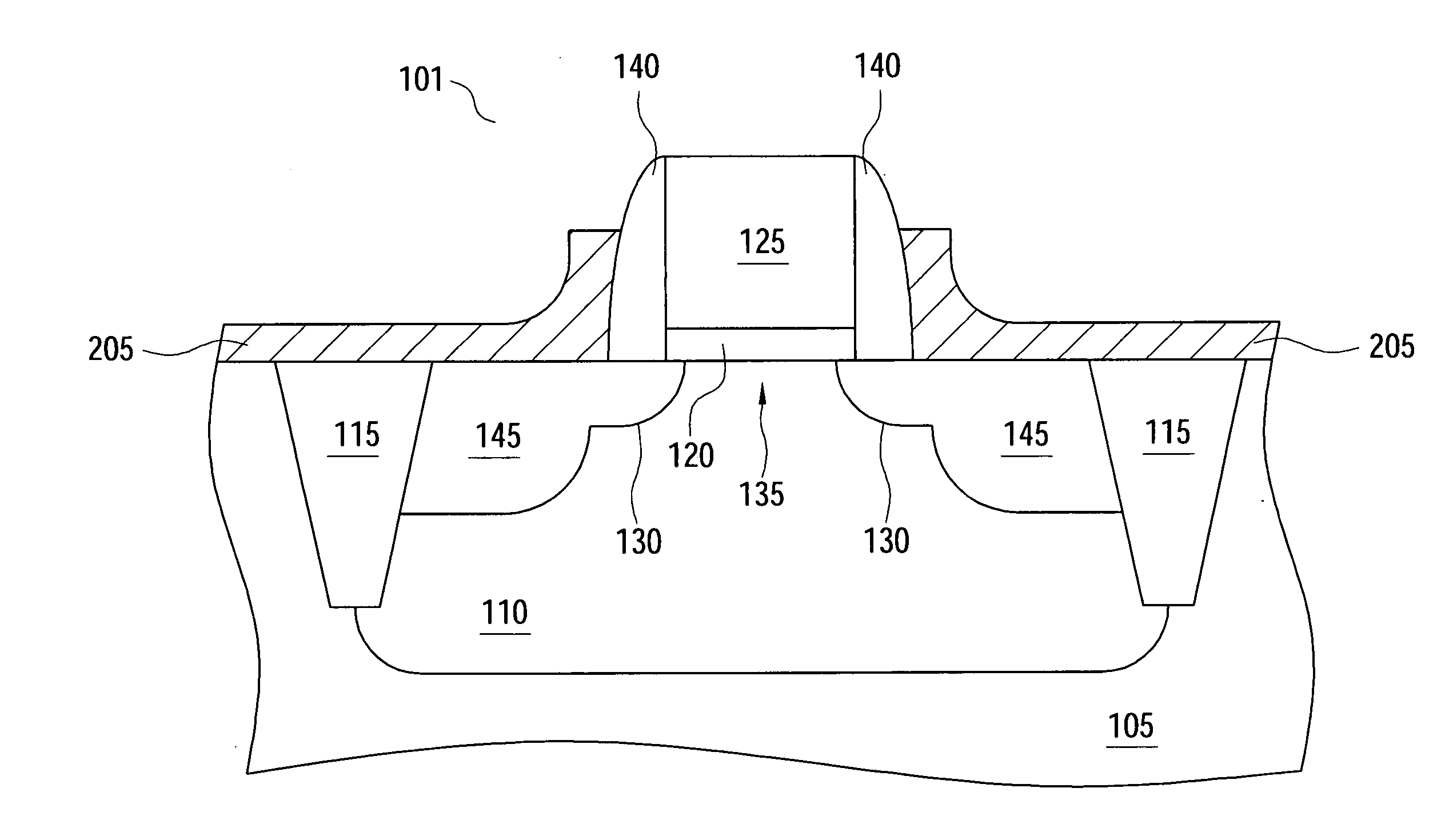
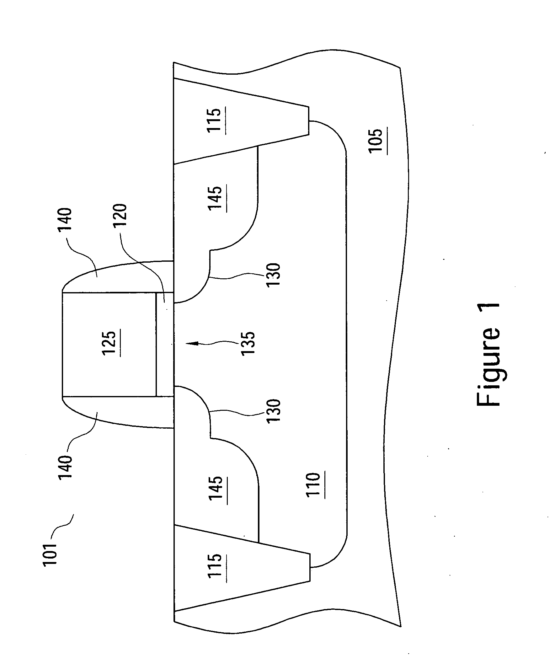
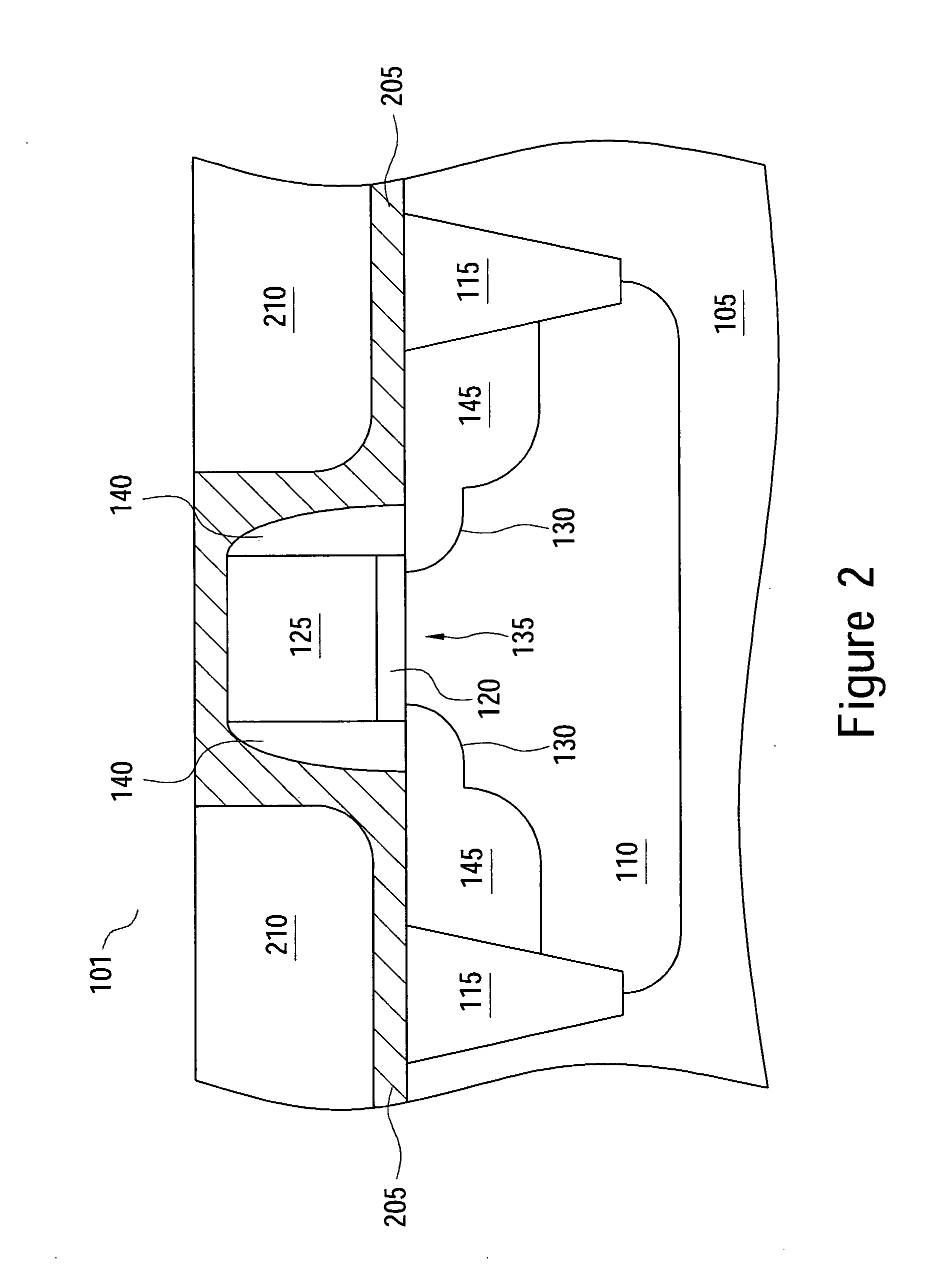
[0014]The making and using of the presently preferred embodiments are discussed in detail below. It should be appreciated, however, that the present invention provides many applicable inventive concepts that can be embodied in a wide variety of specific contexts. The specific embodiments discussed are merely illustrative of specific ways to make and use the invention, and do not limit the scope of the invention. The intermediated stages of manufacturing a preferred embodiment of the present invention are illustrated throughout the various views and illustrative embodiments of the present invention.

[0015]This invention relates generally to semiconductor device fabrication and more particularly to structures and methods for strained transistors. This invention will now be described with respect to preferred embodiments in a specific context, namely the creation of MOS and CMOS devices. Embodiments of this invention are believed to be particularly advantageous when used in this process...


PUM


Abstract

Embodiments of the invention provide a semiconductor fabrication method and a structure for strained transistors. A method comprises forming a stressor layer over a MOS transistor. The stressor layer is selectively etched over the gate electrode, thereby affecting strain conditions within the MOSFET channel region. An NMOS transistor may have a tensile stressor layer, and a PMOS transistor may have compressive stressor layer.

Description

TECHNICAL FIELD[0001]This invention relates generally to semiconductor devices, and, more particularly, to methods and structures for controlling strain in transistors to improve device performance.BACKGROUND[0002]One way to improve transistor performance is through selective application of stress to the transistor channel region. Stress distorts (i.e., strains) the semiconductor crystal lattice, and the distortion in turn affects the band alignment and charge transport properties of the semiconductor. By controlling both the magnitude and distribution of stress in a finished device, manufacturers can increase carrier mobility and improve device performance. There are several approaches for straining the transistor channel region. The details concerning the effects of stress and strain on transistor performance are described in a publication by C. H. Ge et al. in Process-Strained Si (PSS) CMOS Technology Featuring 3D Strain Engineering, Electron Devices Meeting, Dec. 8-10, 2003, IED...

Claims


Application Information

Patent Timeline
Patent Type & Authority Applications(United States)
IPC IPC(8): H01L21/8234
CPCH01L21/823807H01L29/7843H01L29/7833H01L21/28123H01L27/0922H01L29/16H01L29/161
Inventor CHEN, CHIEN-HAOLEE, TZE-LIANG
Owner TAIWAN SEMICON MFG CO LTD
Learn More