Circuit breaker
a circuit breaker and circuit technology, applied in the field of circuit breakers, can solve the problems of large wiring loss, inability to reliably break the fuse, and the fuse was broken, and achieve the effects of small and low-cost, reliably breaking the circuit regardless of operating conditions, and small wiring loss
- Summary
- Abstract
- Description
- Claims
- Application Information
AI Technical Summary
Benefits of technology
Problems solved by technology
Method used
Image

Examples
first embodiment
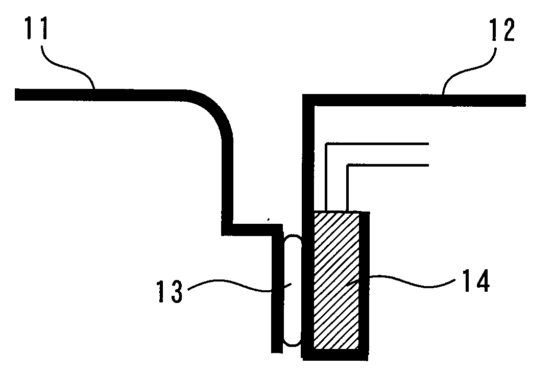
[0022]FIG. 1 is a plan view showing a circuit breaker according to the first embodiment of the present invention. This circuit breaker is used in a power semiconductor device, such as an inverter that passes large current.
[0023]As FIG. 1 shows, a first terminal 11 and a second terminal 12 having favorable electric conductivity, such as copper, are joined to each other with a solder 13. For melting the solder 13, a heater 14 is installed on the back face of the end portion of the second terminal 12. Here, the end portion of the second terminal 12 is bent in a U-shape, and the heater 14 is installed in the U-shaped portion. Thereby heat from the heater 14 can be efficiently supplied to the solder 13, and the heater 14 can be easily fixed. The circumference of the heater 14 is insulated with ceramics or the like.
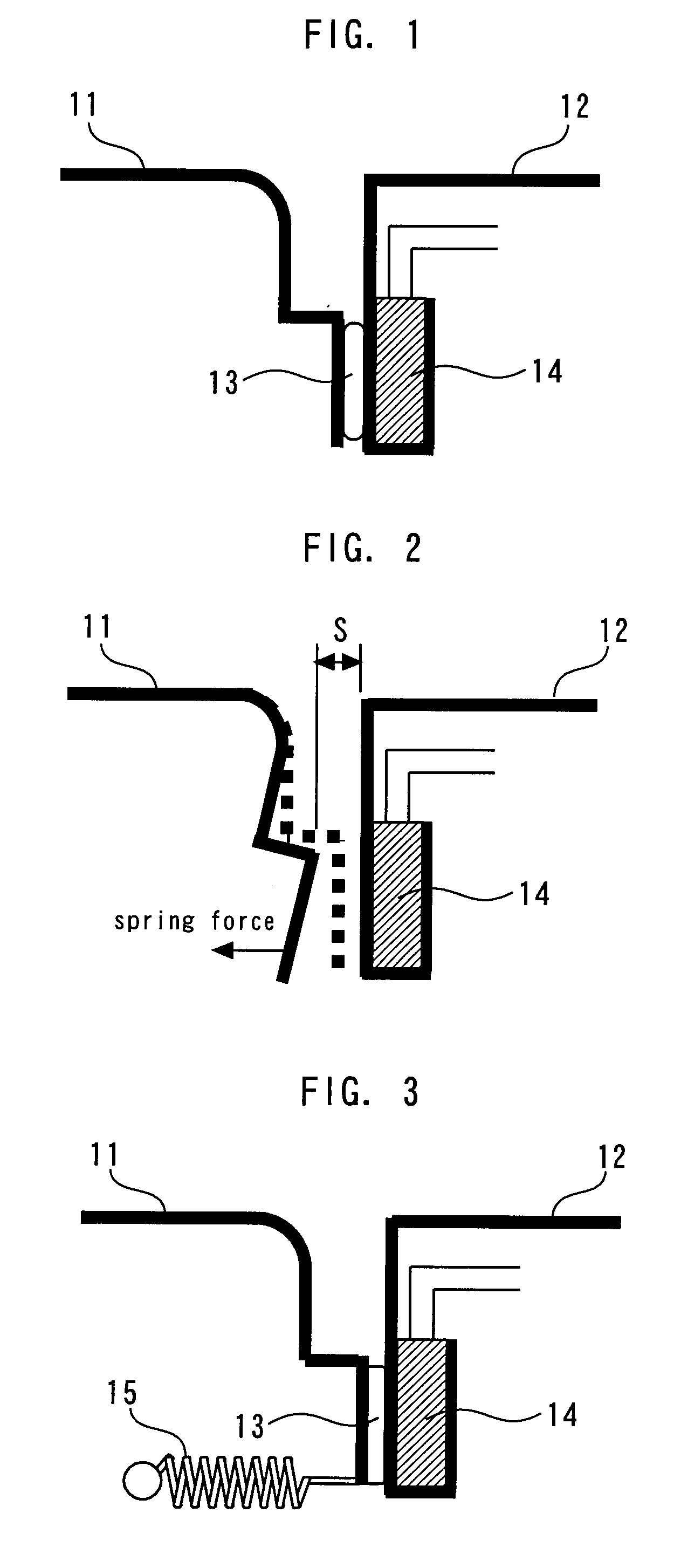
[0024]In the state not joined by solder 13, the first terminal 11 and the second terminal 12 are as shown in FIG. 2. The first terminal 11 has a shape having spring characteris...
second embodiment
[0028]FIG. 3 is a plan view showing a circuit breaker according to the second embodiment of the present invention. In the first embodiment, although the first terminal 11 is separated from the second terminal 12 by the spring force using the spring characteristics of the first terminal 11, in the second embodiment, the spring force is obtained from a spring material 15 other than the first terminal 11 and the second terminal 12. Thereby, without imparting the spring characteristics to the first terminal 11 and the second terminal 12, an effect similar to the effect of the first embodiment can be exerted.
third embodiment
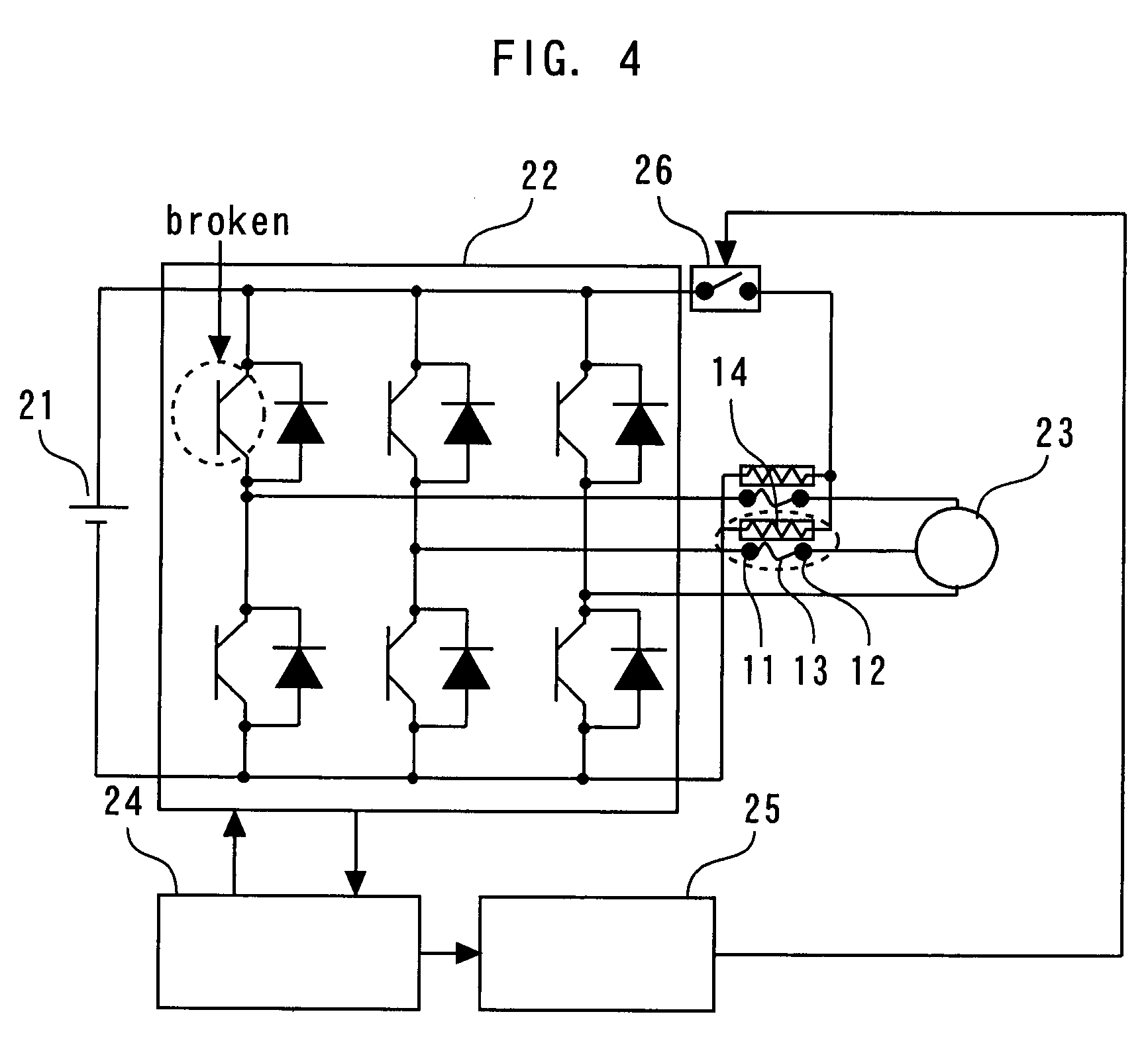
[0029]FIG. 4 is a circuit diagram showing a power semiconductor device according to the third embodiment of the present invention. This power semiconductor device has a circuit to invert the current from the battery power source 21 into AC using an inverter circuit 22, and to drive a three-phase motor 23. It has also an inverter control circuit 24 to control the inverter circuit 22, a breaking control circuit 25, a switch 26, and a circuit breaker similar to the circuit breaker of the first or second embodiment. The first terminal 11 and the second terminal 12 are connected to the three-phase motor 23 and the inverter circuit 22 to drive the three-phase motor 23, respectively.
[0030]When the inverter control circuit 24 detects the abnormality of the inverter circuit 22, it transmits signals to the breaking control circuit 25, and upon the receipt of the signals, the breaking control circuit 25 outputs ON signal to the switch 26. When the ON signal from the breaking control circuit 25...
PUM
 Abstract
Description
Claims
Application Information
 - R&D Engineer
- R&D Manager
- IP Professional
- Industry Leading Data Capabilities
- Powerful AI technology
- Patent DNA Extraction
Browse by: Latest US Patents, China's latest patents, Technical Efficacy Thesaurus, Application Domain, Technology Topic.
© 2024 PatSnap. All rights reserved.Legal|Privacy policy|Modern Slavery Act Transparency Statement|Sitemap