Circuit and method for reducing electromagnetic interference

a technology of electromagnetic interference and circuit, applied in the field of electronic circuits, can solve problems such as electromagnetic radiation, adversely affecting other circuit components either in the same system or in the other system, and reducing the size of the system of the circui

Active Publication Date: 2007-12-20
SEMICON COMPONENTS IND LLC
View PDF18 Cites 48 Cited by
  • Summary
  • Abstract
  • Description
  • Claims
  • Application Information

AI Technical Summary

Problems solved by technology

One type of stress that interferes with the proper operation of an electrical system is electromagnetic radiation.
In addition to being affected by EMI, the electronic components also radiate electromagnetic signals, which may adversely affect other circuit components either in the same system or in other systems.
As the desire for smaller more compact systems has increased, systems manufacturers have decreased the sizes of their systems, which increases

Method used


Image

  • Circuit and method for reducing electromagnetic interference
  • Circuit and method for reducing electromagnetic interference
  • Circuit and method for reducing electromagnetic interference

Examples


Embodiment Construction

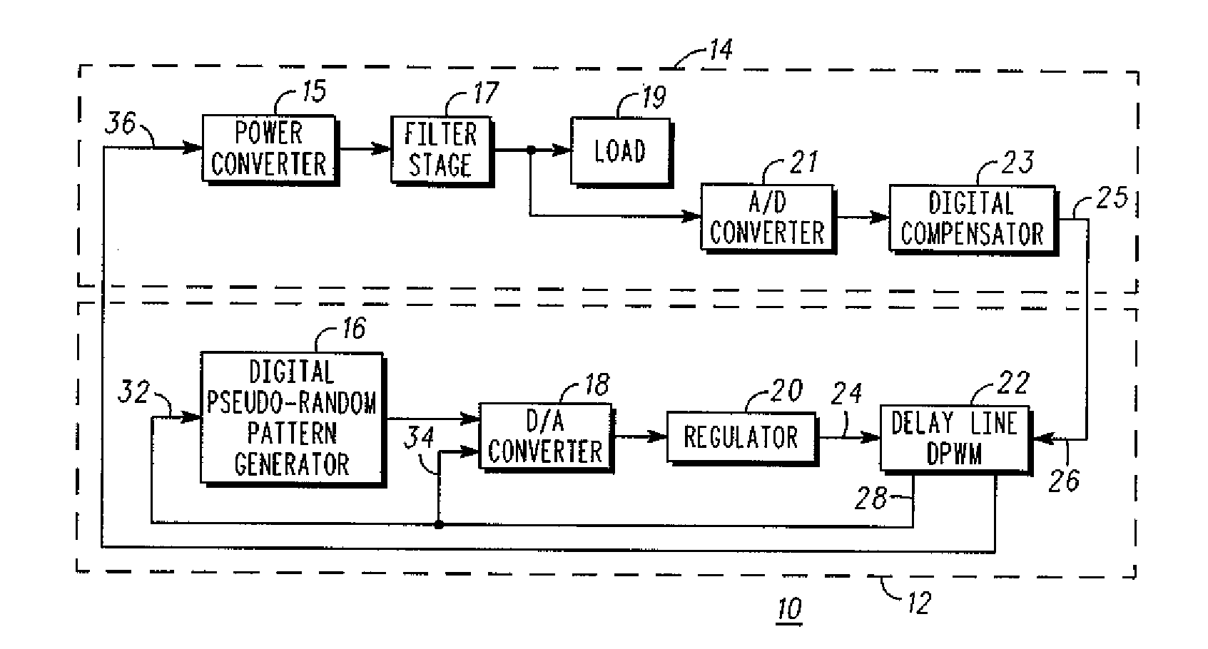
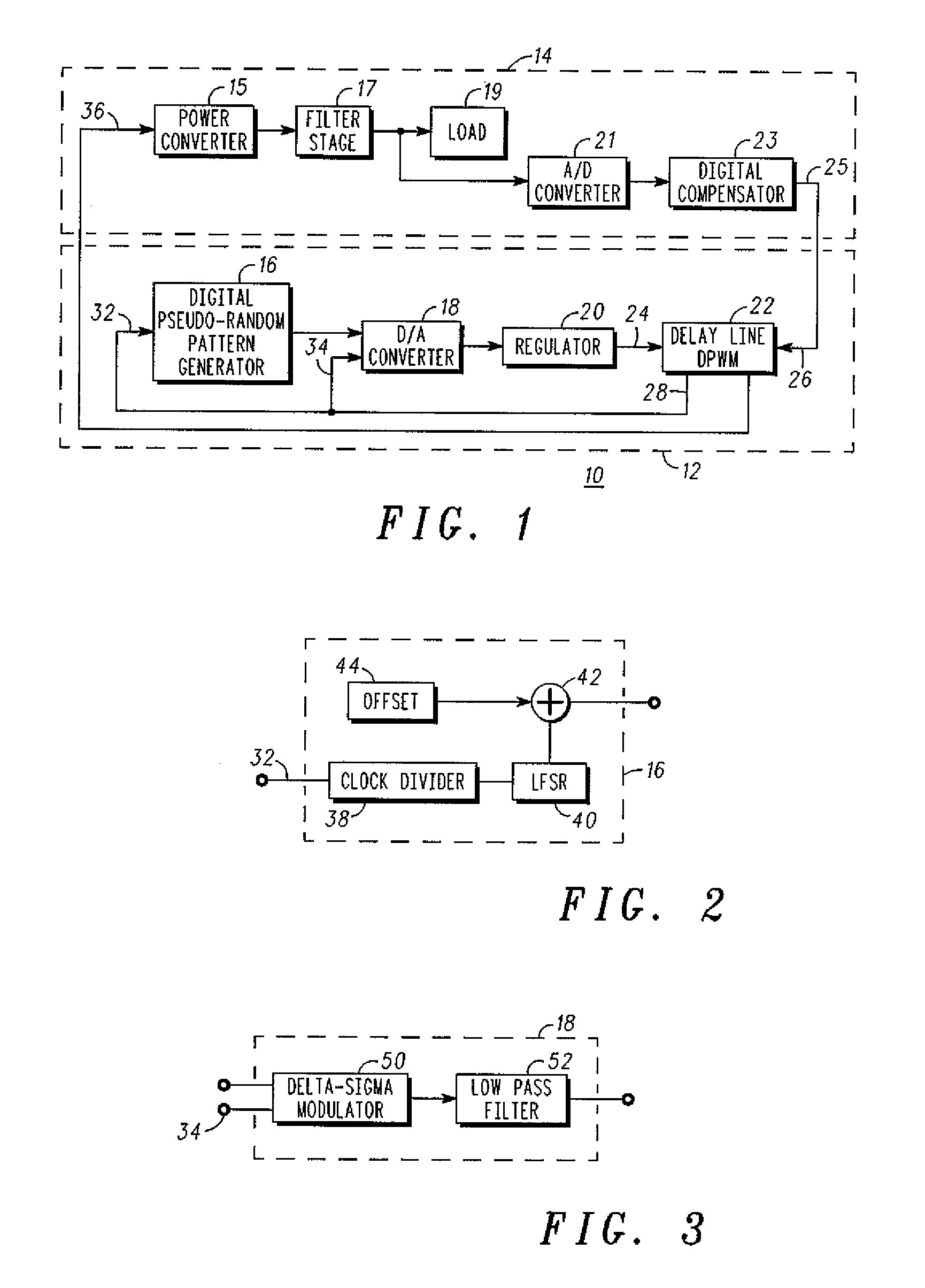
[0012] In general, the present invention includes a method and circuit for reducing or inhibiting electromagnetic interference using a digital circuit architecture and spread spectrum clock generation. In accordance with an embodiment of the present invention, the switching frequency of a circuit is varied using a digital pseudo-random pattern generator and a delay-line digital pulse width modulator to create a digital spread spectrum, which is also referred to as a randomized pulse width modulation signal. The pseudo-random pattern generator transmits pseudo-random digital codes to a noise shaping digital-to-analog converter. The delay-line digital pulse width modulator generates a system clock signal having a frequency that is controlled by an analog supply voltage for the delay-line whose value is randomized around an average value. This varying clock frequency spreads the radiated and conducted EMI over a wide range of frequencies in a random fashion rather than at a constant fr...


PUM


Abstract

A spread spectrum system having a self-oscillating delay-line digital pulse width modulator and a method for mitigating electromagnetic interference. The spread spectrum system has a pseudo-random pattern generator connected to a digital-to-analog converter, which in turn is connected to a linear regulator. The linear regulator receives a reference voltage from the digital-to-analog converter and creates a frequency varying voltage that serves as an input voltage for delay elements of a delay-line based digital pulse width modulator. In response to frequency varying input signal, the delay-line based digital pulse width modulator generates a frequency varying voltage that is input to a switching network to vary its switching frequency.

Description

FIELD OF THE INVENTION [0001] This invention relates, in general, to electronic circuits and, more particularly, to spread spectrum operation of digitally controlled power converters. BACKGROUND OF THE INVENTION [0002] Systems such as automotive, aviation, telecommunications, consumer electronics, etc. comprise many elements that may be adversely affected by physical, environmental, and electrical stresses. These elements include electronic components, passive circuit elements, and interconnect structures. One type of stress that interferes with the proper operation of an electrical system is electromagnetic radiation. This type of stress is also referred to as Electromagnetic Interference (“EMI”). In addition to being affected by EMI, the electronic components also radiate electromagnetic signals, which may adversely affect other circuit components either in the same system or in other systems. As the desire for smaller more compact systems has increased, systems manufacturers have...

Claims


Application Information

Patent Timeline
IPC IPC(8): H03M7/00
CPCH02M1/44H02M3/157H03K3/0315H03K3/84H04B2215/067H03M1/502H03M1/60H04B15/02H03M1/14H02M7/539
Inventor NG, WAI TUNGTRESCASES, OLIVIER
Owner SEMICON COMPONENTS IND LLC
Why Eureka
Try Eureka