Semiconductor memory device

a memory device and semiconductor technology, applied in the field of semiconductor memory devices, can solve the problems of the entire size of the memory device, the speed of the operation deterioration,

Inactive Publication Date: 2007-12-20
SANYO ELECTRIC CO LTD
View PDF2 Cites 0 Cited by
  • Summary
  • Abstract
  • Description
  • Claims
  • Application Information

AI Technical Summary

Benefits of technology

[0014]The preferred embodiments of the present invention have been developed in view of the above-mentioned and / or other problems in the related art. The preferred embodiments of the present invention can significantly improve upon existing methods and / or apparatuses.
[0015]Among other potential advantages, some embodiments can provide a semiconductor memory device with less crosstalk.
[0016]Among other potential advantages, some embodiments can provide a divided precharge type semiconductor memory device capable of decreasing crosstalk without increasing the size of the device even if data lines are long.
[0023]With this structure, it becomes possible to prevent the electrical potentials of the data lines or complementary data lines arranged at both sides of the data line or the complementary data line from becoming L-potentials. As a result, the capacity between the data lines decreases, which in turn can suppress the effects of crosstalk without increasing the distance between the data lines.
[0025]Furthermore, it is preferable that half of the plural pairs of the complementary data lines are crossed one time at a longitudinal intermediate position of the data line and the other half thereof remains non-crossed. With this structure, the effects of crosstalk can be effectively suppressed.

Problems solved by technology

In this case, if all of the memory cells are to be precharged, the operating speed deteriorates.
This causes the entire size of the memory device.

Method used


Image

  • Semiconductor memory device
  • Semiconductor memory device
  • Semiconductor memory device

Examples


Embodiment Construction

[0034]In the following paragraphs, some preferred embodiments of the present invention will be described by way of example and not limitation. It should be understood based on this disclosure that various other modifications can be made by those in the art based on these illustrated embodiments.

[0035]A semiconductor memory device according to an embodiment of the present invention will be explained with reference to the attached drawings.

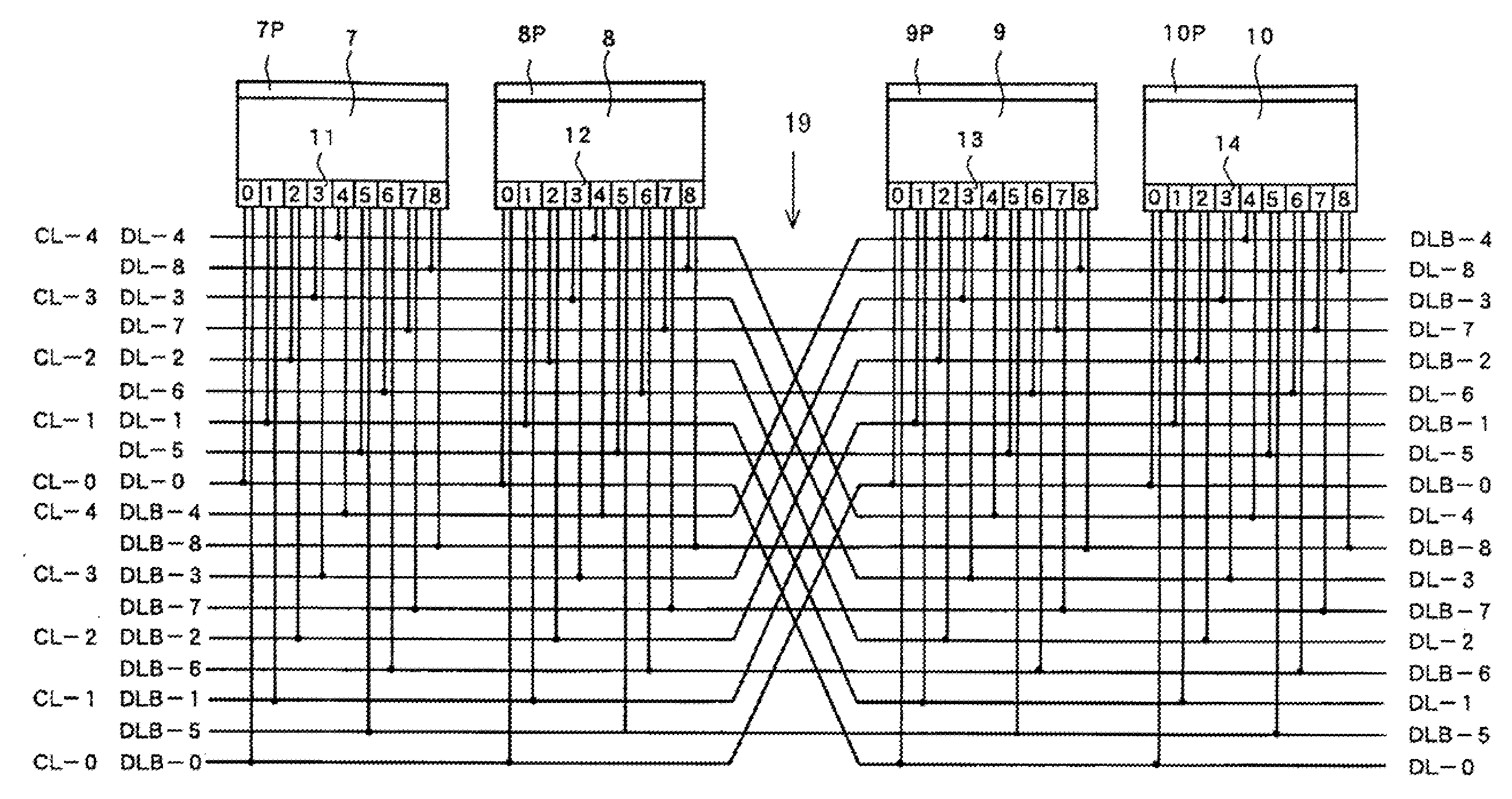
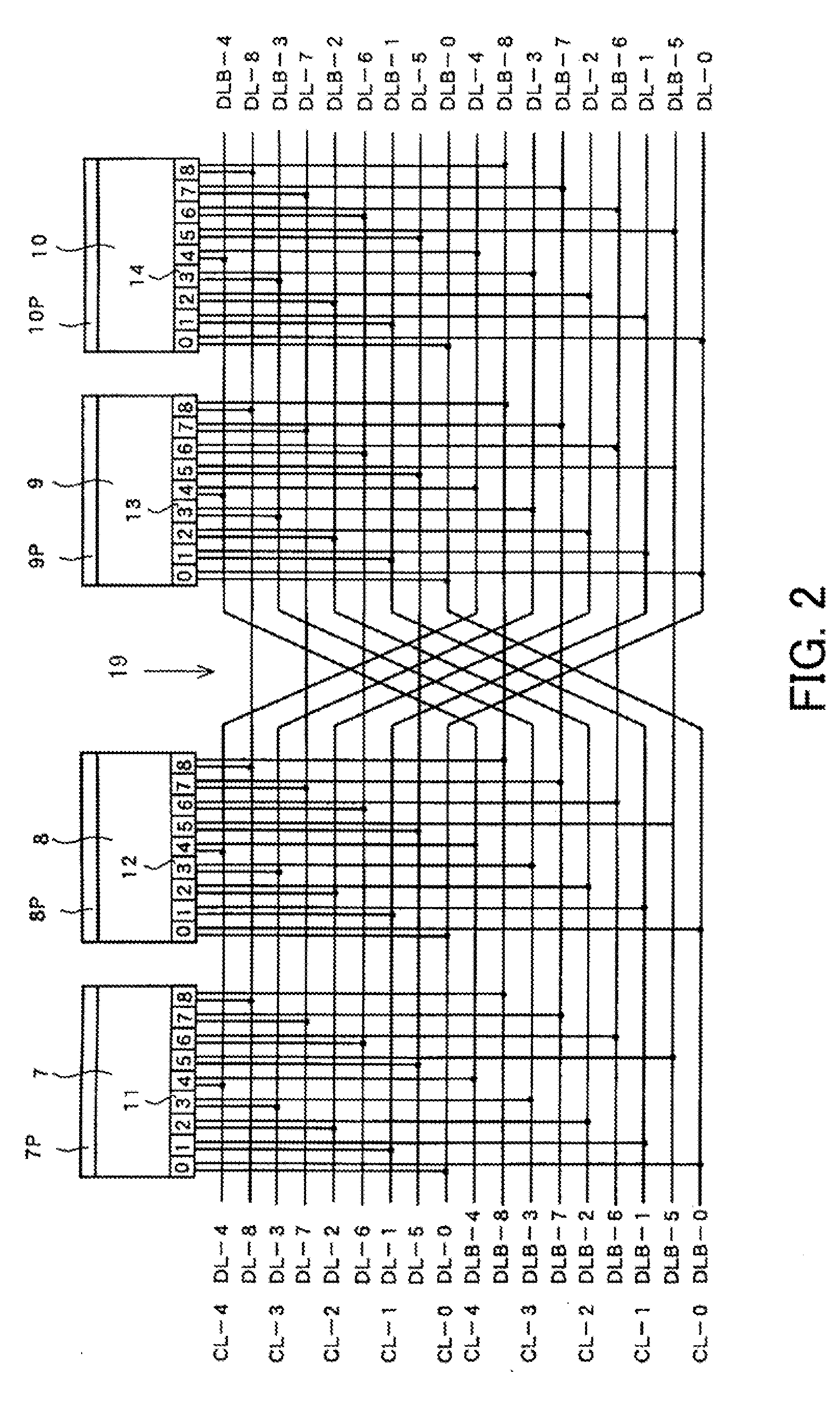
[0036]Initially, a memory cell constituting a semiconductor memory device according to an embodiment of the present invention will be explained FIG. 1 shows an example of an SRAM used as a memory cell.

[0037]This memo cell includes a first inverter 1, a second inverter 2, a first access transistor 3 and a second access transistor 4. The first inverter 1 and the second inverter 2 constitute a latch circuit in which the input and the output are cross-linked. The gate of the first access transistor 3 and that of the second access transistor 4 are connec...


PUM


Abstract

According to some preferred embodiments of the present invention, a semiconductor memory device includes an array of memory cells and plural pairs of complementary bit lines, each pair of the complementary bit lines being connected to the memory cells arranged in the same column. The array is divided into plural memory blocks each including plural memory cells arranged in the same column. The corresponding complementary bit lines of the plural memory blocks are connected to corresponding common complementary data lines, respectively. Some pairs of the complementary data lines are crossed at least one time so that the complementary data lines of each pair of the some pairs of the complementary data lines are reversed in position and that the crossed data line and a non-cross data line are arranged alternately whereby crosstalk to be generated between adjacent data lines are reduced.

Description

[0001]This application claims priority under 35 U.S.C. §119 to Japanese Patent Application No. 2006-162703 filed on Jun. 12, 2006, the entire disclosure of which is incorporated herein by reference in its entirety.BACKGROUND OF THE INVENTION[0002]1. Field of the Invention[0003]The present invention relates to a semiconductor memory device. More specifically, some preferred embodiments of the present invention relate to a semiconductor memory device having SRAMs (Static Random Access Memories).[0004]2. Description of the Related Art[0005]The following description sets forth the inventor's knowledge of related art and problems therein and should not be construed as an admission of knowledge in the prior art.[0006]As one of semiconductor memory devices, a semiconductor memory device having SRAMs is known. An SRAM is one of random access memories (RAM) capable of performing writing and reading operations without requiring refresh operations so long as a power supply voltage is being app...

Claims


Application Information

Patent Timeline
Patent Type & Authority Applications(United States)
IPC IPC(8): G11C7/00G11C11/00G11C7/02
CPCG11C5/063G11C11/417G11C7/18G11C7/02
Inventor MITSUYA, KAZUYUKI
Owner SANYO ELECTRIC CO LTD
Why Eureka
Try Eureka