Printed wiring board

a technology of printed wiring and printed boards, applied in the direction of printed circuit manufacturing, printed circuit aspects, high frequency circuit adaptations, etc., can solve the problem that high-speed signal transmission cannot be realized withou

Inactive Publication Date: 2008-01-03
FUJITSU LTD
View PDF3 Cites 12 Cited by
  • Summary
  • Abstract
  • Description
  • Claims
  • Application Information

AI Technical Summary

Benefits of technology

[0006] It is accordingly an object of the present invention to provide a printed wiring board significantly contributing to realization of a high-speed signal transmission.
[0009] In addition, the inner via serving as a ground is located inside the outer via serving as a signal line. The impedance matching can reliably be established. This results in a reliable signal transmission between components mounted on the printed wiring board. The printed wiring board allows the transmission of a high speed exceeding several GHz.

Problems solved by technology

However, a high-speed signal transmission cannot be realized without the ground via.

Method used


Image

  • Printed wiring board
  • Printed wiring board
  • Printed wiring board

Examples


Embodiment Construction

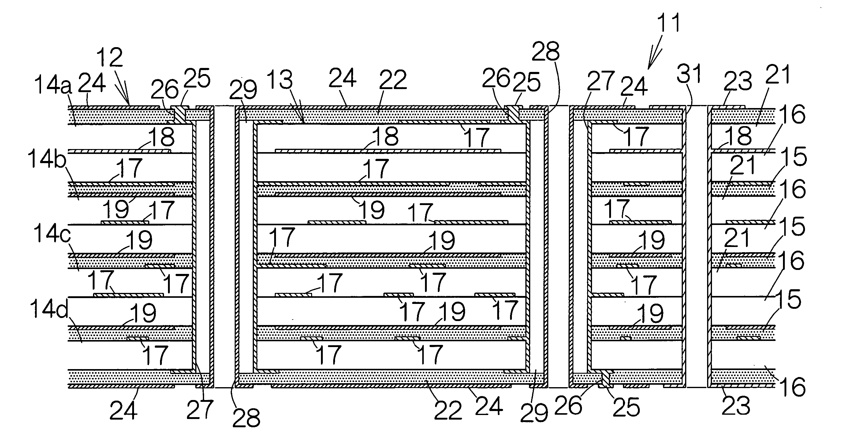
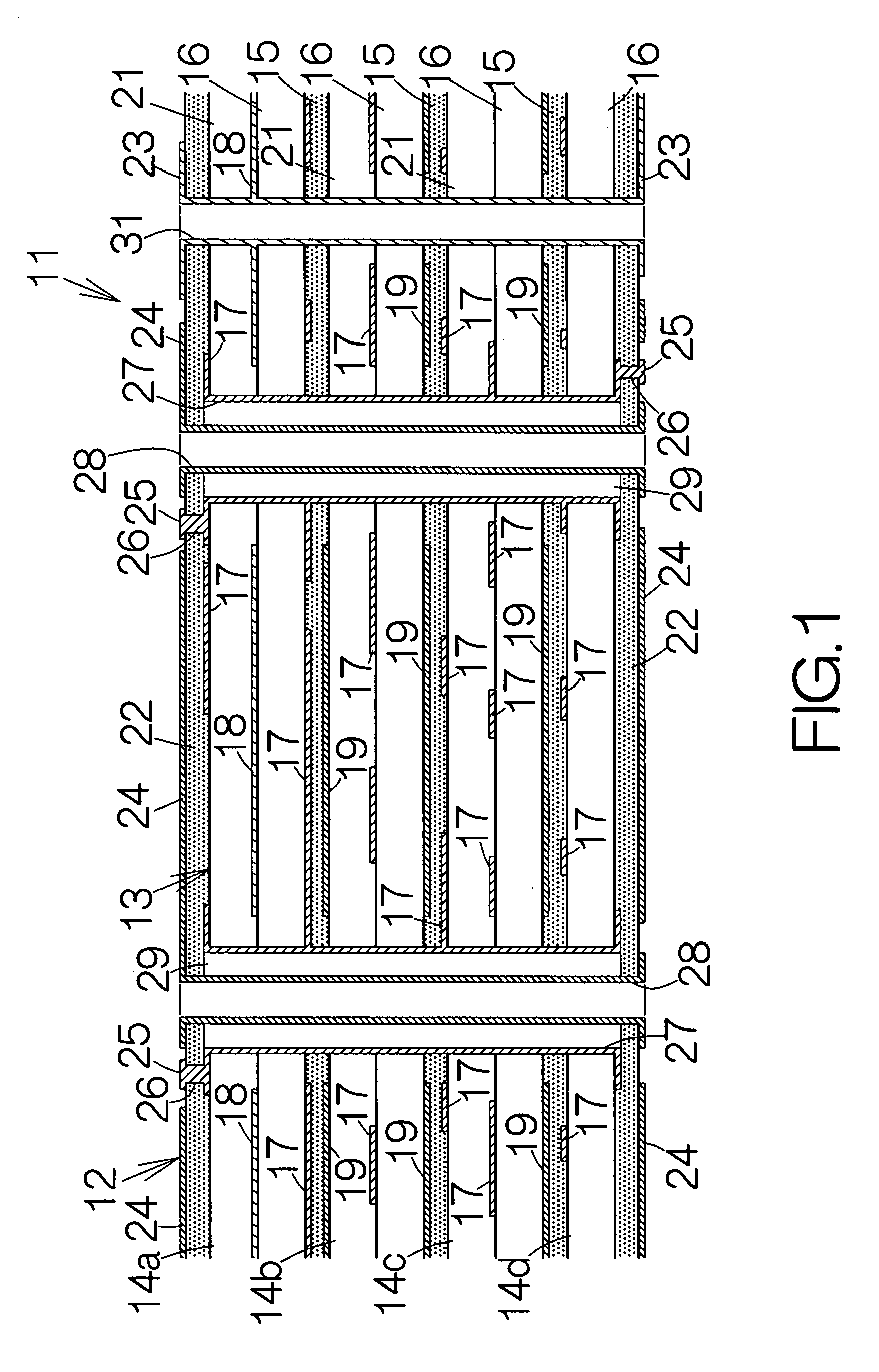
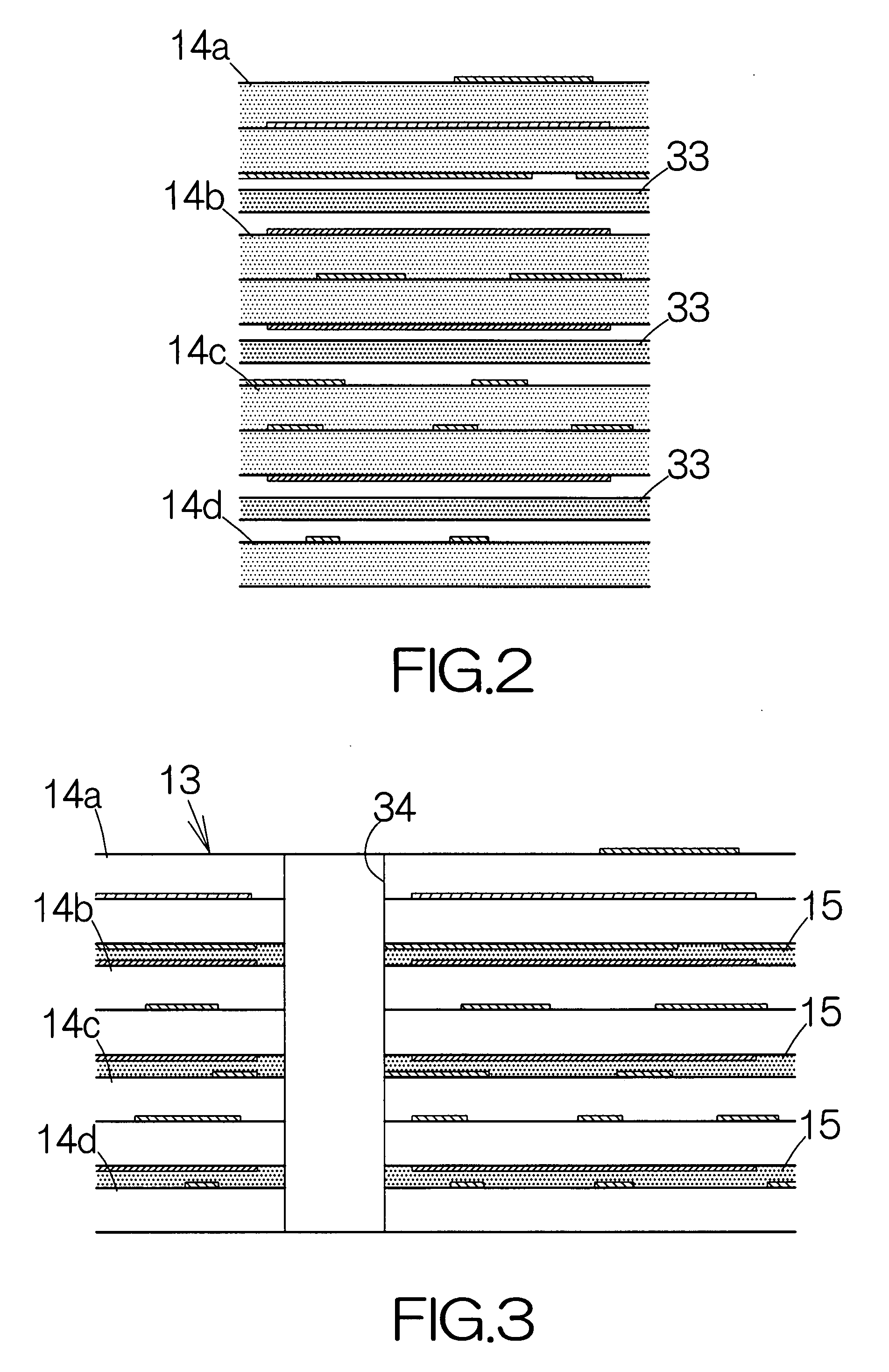
[0020]FIG. 1 illustrates a printed wiring board unit according to an embodiment of the present invention. The printed wiring board unit 11 includes a printed wiring board 12 having a multilayered structure. The printed wiring board 12 includes a board 13. Component substrates 14a, 14b, 14c, 14d are incorporated in the board 13. The component substrates 14a, 14b, 14c, 14d are overlaid on one another. An insulating resin layer 15 such as a prepreg is interposed between the adjacent ones of the component substrates 14a, 14b, 14c, 14d. The insulating resin layers 15 serve to bond the adjacent component substrates 14a, 14b, 14c, 14d to each other.

[0021] The component substrates 14a-14d each include a core substrate 16. The core substrate 16 is made of a resin material, a ceramic material, or the like. The core substrate 16 has a rigidity sufficient to maintain its shape by itself.

[0022] A signal line pattern or patterns 17, a power supply pattern or patterns 18 and a ground pattern or ...


PUM


Abstract

A signal line, a power supply pattern and a ground layer are formed within a board. An outer via and an inner via are formed within the board. The outer via is connected to the signal line. The inner via is connected to the ground layer. The outer via serves as a signal line. The inner via serves as a ground. The signal line within a printed wiring board is connected to the outer via without interruption by a ground. The signal lines can spread within the printed wiring board in a complicated pattern as compared with a conventional pattern. Moreover, the impedance matching can reliably be established.

Description

BACKGROUND OF THE INVENTION [0001] 1. Field of the Invention [0002] The present invention relates to a printed wiring board. [0003] 2. Description of the Prior Art [0004] In general, wiring patterns are formed on the front and back surfaces of a substrate for signal lines in a printed wiring board. The signal lines on the front and back surfaces are connected to each other through a via penetrating through the substrate, for example. A ground via is also formed outside the via for the signal lines. The ground via is coaxial with the via for the signal lines. Coaxial cable lines are established in the substrate in this manner. The ground via serves to trap noise of the signal lines. [0005] Proposed is a so-called multilayered printed wiring board. Double-sided wiring boards are overlaid on one another in sequence. If the aforementioned coaxial vias are formed in such a multilayered structure, the ground via prevents connection between signal lines inside the multilayered wiring board...

Claims


Application Information

Patent Timeline
Patent Type & Authority Applications(United States)
IPC IPC(8): H05K1/11H01R12/04
CPCH05K1/0251H05K1/115H05K2201/09809H05K3/4602H05K3/429H05K1/02
Inventor NAKAMURA, NAOKI
Owner FUJITSU LTD
Why Eureka
Try Eureka