Mixed analog and digital pixel for high dynamic range readout

a technology of high dynamic range, which is applied in the field of improved cmos imaging sensors having mixed analog and digital pixel readout, can solve the problems of limited maximum optical signal that a pixel can detect, unsuitable, and inability to improve the ability of imagers to capture very bright and very dark objects in the same scene, so as to achieve the effect of large pixel dynamic range without compromising low-light performan

Active Publication Date: 2008-01-03
INFRARED NEWCO
View PDF5 Cites 45 Cited by
  • Summary
  • Abstract
  • Description
  • Claims
  • Application Information

AI Technical Summary

Benefits of technology

[0024]Briefly stated, the present invention provides an improved CMOS pixel with a combination of analog and digital readouts to provide a large pixel dynamic range without compromising low-light performance. The pixel design uses a comparator to test the value of an accumulated charge at a series of exponentially increasing exposure time intervals. A one-bit output value of the test is read out of the pixel (digitally) at each of the exponentially increasing exposur

Problems solved by technology

The maximum optical signal that a pixel can detect is limited by the charge accumulation capacity of the integration capacitor.
They do not, however, improve an imager's ability to capture very bright and very dark objects in the same scene.
They are not suitable, therefore, for these high dynamic range applications.
Unfortunately, it also reduces the conversion gain of the pixel which reduces sensitivity of the imager and therefore the signal to noise ratio at low light levels.
While such devices can achieve very high dynamic range, they suffer from poor sensitivity, low signal to noise ratio and exhibit high levels of fixed pattern noise.
It also suffers from high power dissipation because the precision comparator is “always on”.
There are, however, a number of probl

Method used


Image

  • Mixed analog and digital pixel for high dynamic range readout
  • Mixed analog and digital pixel for high dynamic range readout
  • Mixed analog and digital pixel for high dynamic range readout

Examples


Embodiment Construction

[0035]The following detailed description illustrates the invention by way of example and not by way of limitation. The description enables one skilled in the art to make and use the invention, and describes several embodiments, adaptations, variations, alternatives, and uses of the invention, including what is presently believed to be the best mode of carrying out the invention.

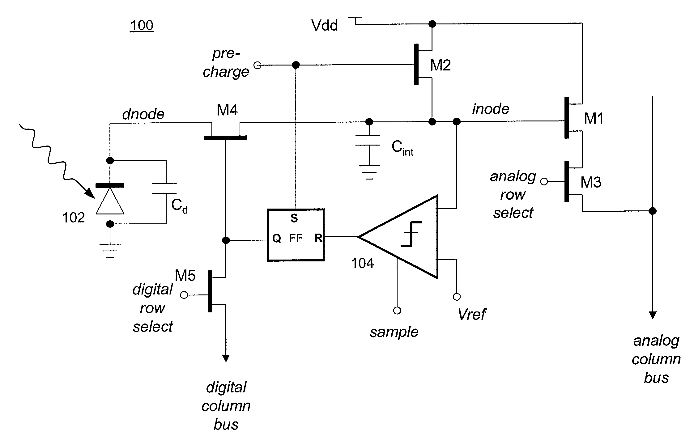
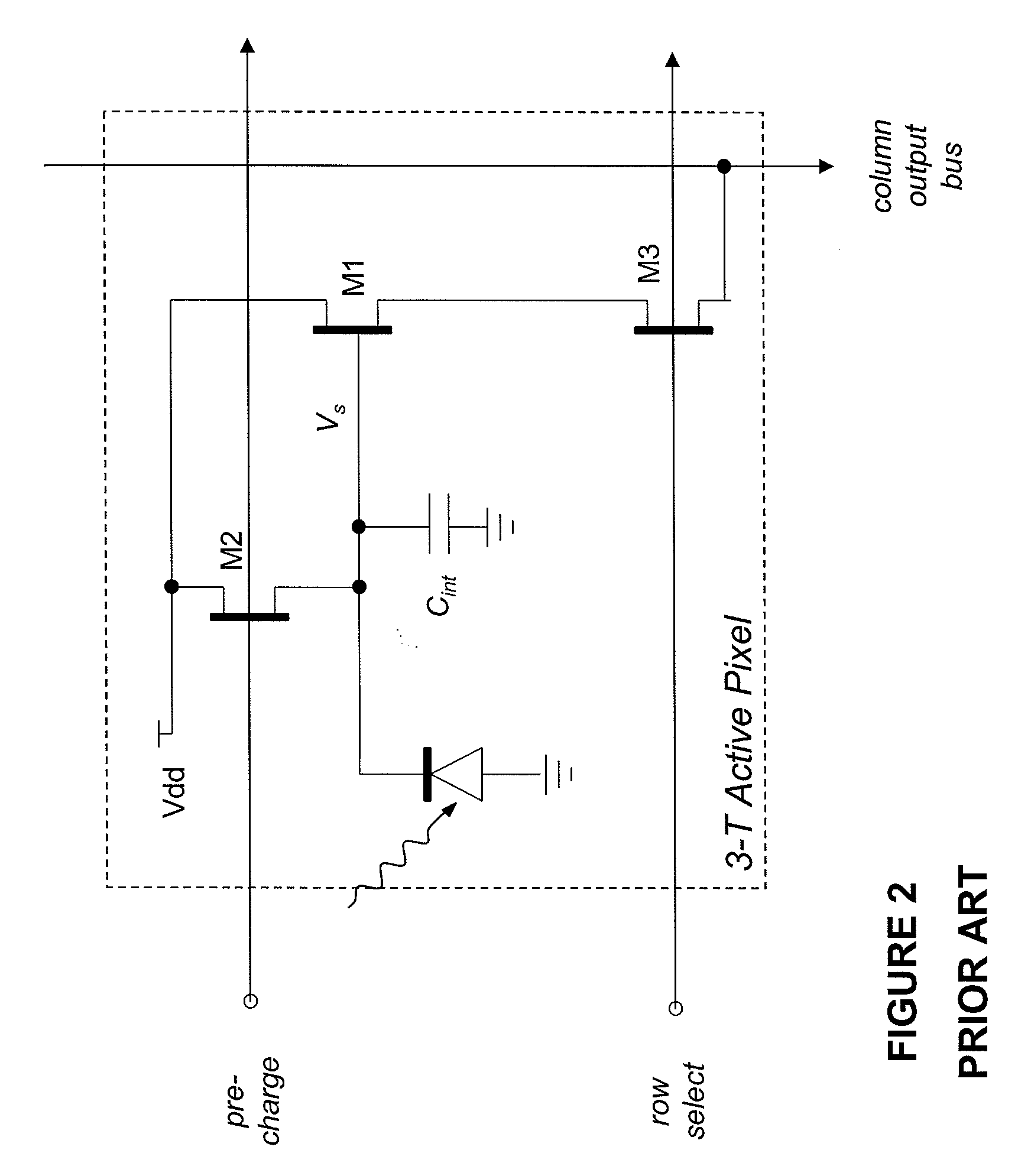
[0036]In general, an improved CMOS pixel of the present invention utilizes a combination of analog and digital readout to provide a large pixel dynamic range without compromising low-light performance using a comparator to test the value of accumulated charge at a series of exponentially increasing exposure times. Analog to digital conversion is not performed within the pixel. The test is used to stop the integration of photocurrent once the accumulated analog voltage has reached a predetermined threshold. The one-bit output value of the test is read out of the pixel (digitally) at each of the exponentially i...


PUM


Abstract

An improved CMOS pixel with a combination of analog and digital readouts to provide a large pixel dynamic range without compromising low-light performance using a comparator to test the value of an accumulated charge at a series of exponentially increasing exposure times. The test is used to stop the integration of photocurrent once the accumulated analog voltage has reached a predetermined threshold. A one-bit output value of the test is read out of the pixel (digitally) at each of the exponentially increasing exposure periods. At the end of the integration period, the analog value stored on the integration capacitor is read out using conventional CMOS active pixel readout circuits.

Description

CROSS-REFERENCE TO RELATED APPLICATIONS[0001]Not Applicable.STATEMENT REGARDING FEDERALLY SPONSORED RESEARCH[0002]Not Applicable.BACKGROUND OF THE INVENTION[0003]The present invention is related generally to CMOS imaging sensors, and in particular to an improved CMOS imaging sensor having mixed analog and digital pixel readout for high dynamic range.[0004]Solid state image sensors (“imagers”) are important in a wide variety of applications including professional and consumer video and still image photography, remote surveillance for security and safety, astronomy and machine vision. Imagers that are sensitive to non-visible radiation, for example infrared radiation, are used in some other applications including night vision, camouflage detection, non-visible astronomy, art conservation, medical diagnosis, ice detection (as on roads and aircraft), and pharmaceutical manufacturing.[0005]An image sensor comprises a two-dimensional array of photosensitive elements (pixels) in combinatio...

Claims


Application Information

Patent Timeline
IPC IPC(8): H01L27/00H04N5/353H04N5/355H04N5/374H04N5/378
CPCH04N5/3559H04N5/3742H04N5/3745H04N25/59H04N25/77H04N25/57H04N25/75H04N25/767
Inventor ACKLAND, BRYAN
Owner INFRARED NEWCO
Why Eureka
Try Eureka