
Semiconductor device having terminals

a technology of semiconductor devices and terminals, which is applied in the direction of semiconductor devices, semiconductor/solid-state device details, printed circuit board receptacles, etc., can solve the problems of large cost of packaging prototyping, different mold manufacturing, time-consuming, etc., and achieve the effect of reducing the restriction on the layout inside the enclosur

Active Publication Date: 2008-01-03
MITSUBISHI ELECTRIC CORP
View PDF7 Cites 8 Cited by
  • Summary
  • Abstract
  • Description
  • Claims
  • Application Information

AI Technical Summary

Benefits of technology

[0008]An object of the present invention is to provide a semiconductor device that can adapt to variation in shape and arrangement of terminals attributable to differences in circuit configuration and the like of the semiconductor apparatuses, and that can reduce restriction on the layout inside the enclosure.
[0010]According to the semiconductor device of the present invention, it is possible to adapt to variation in shape and arrangement of the terminals attributable to the differences in circuit configuration and the like of the semiconductor apparatuses, and it is also possible to reduce restriction on the layout inside the enclosure.

Problems solved by technology

This however requires a large cost for prototyping of the packages, and for manufacture of different molds for mass-production thereof.
Further, there is a need to address problems that would occur in the packages of various configurations, which causes delay in development, and requires time to verify those packages.
With the power semiconductor device of Japanese Patent Laying-Open No. 09-008191, however, the terminal member is arranged at the upper surface of the casing, which would largely restrict the layout inside the package.

Method used


Image

  • Semiconductor device having terminals
  • Semiconductor device having terminals
  • Semiconductor device having terminals

Examples


first embodiment

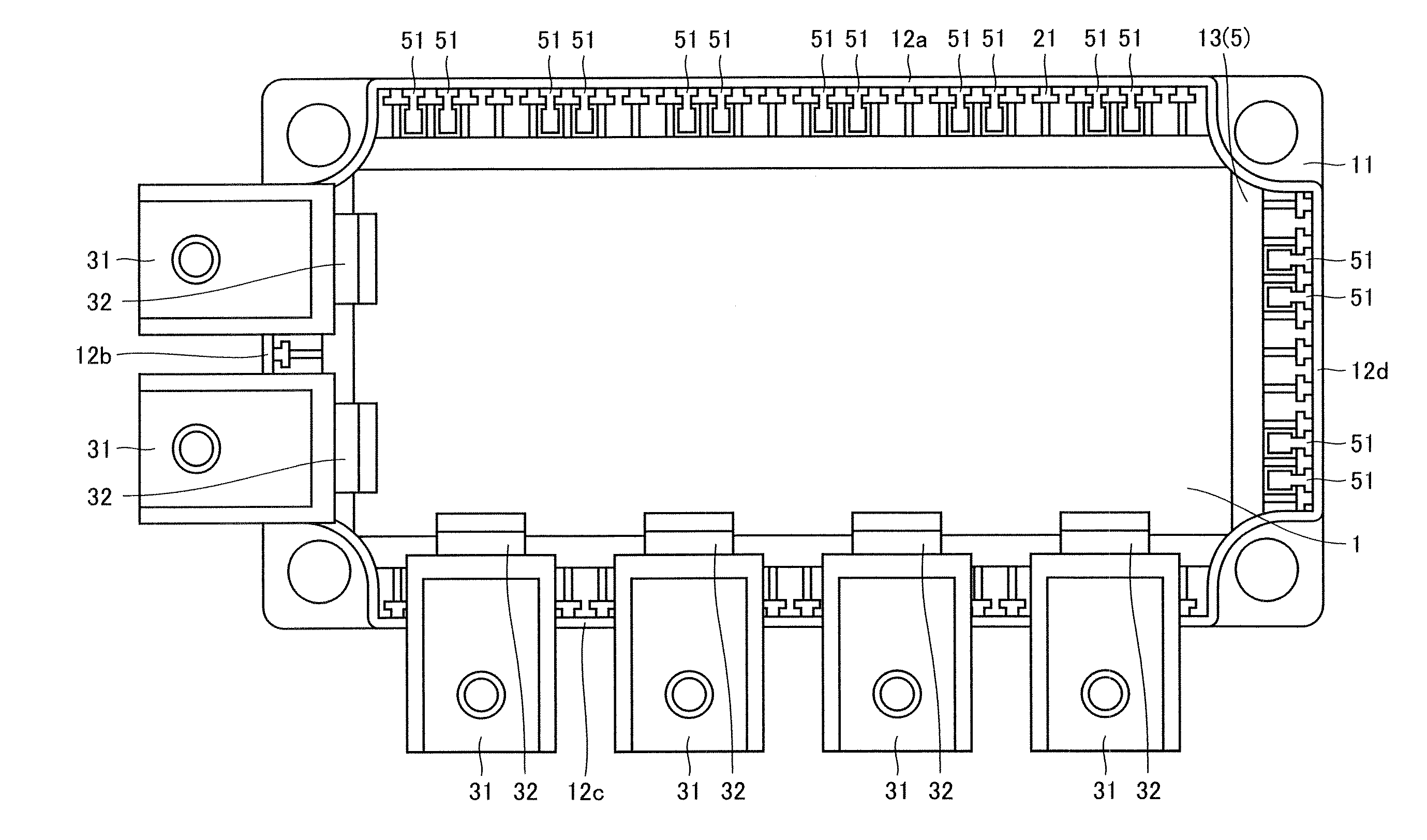
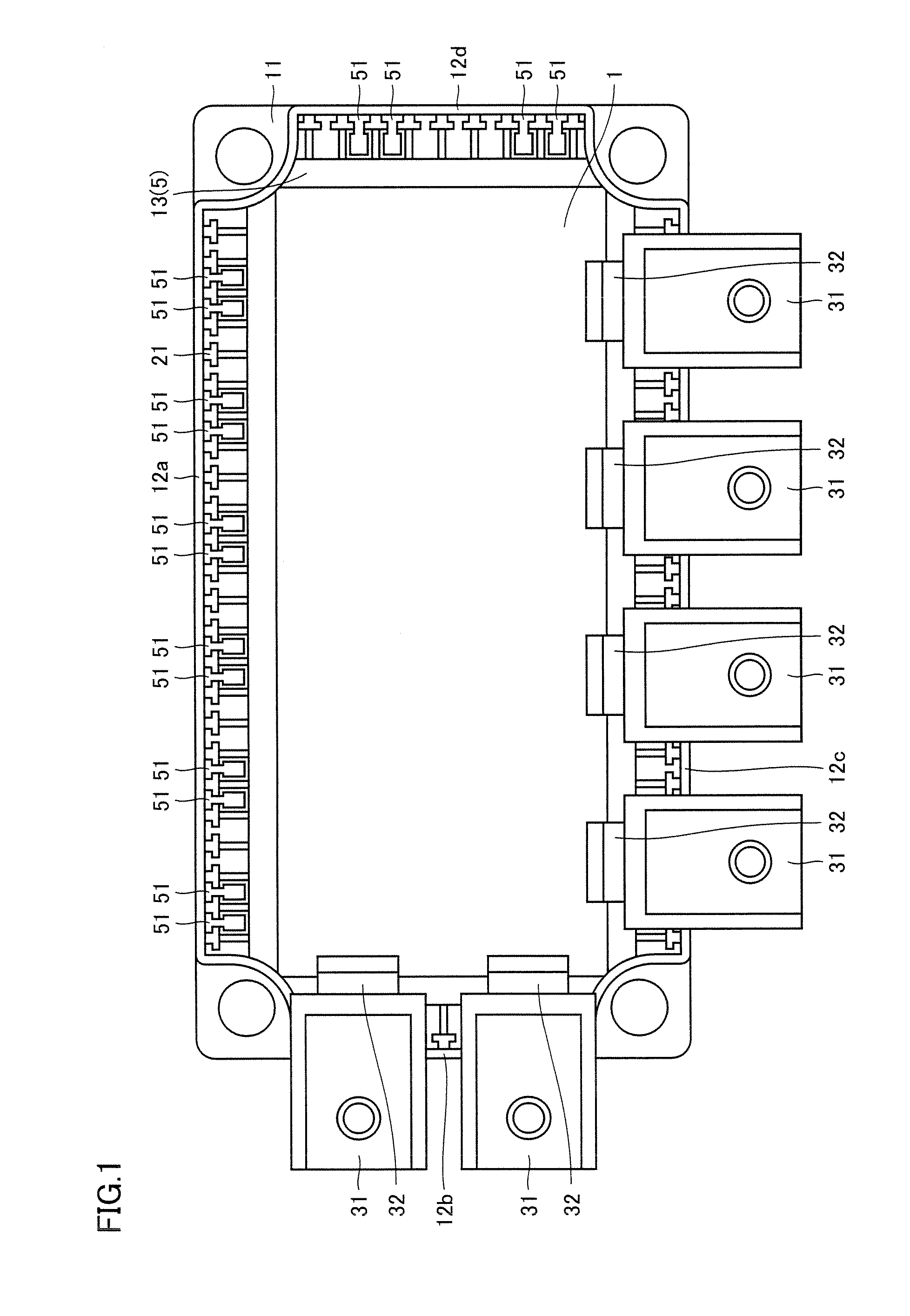
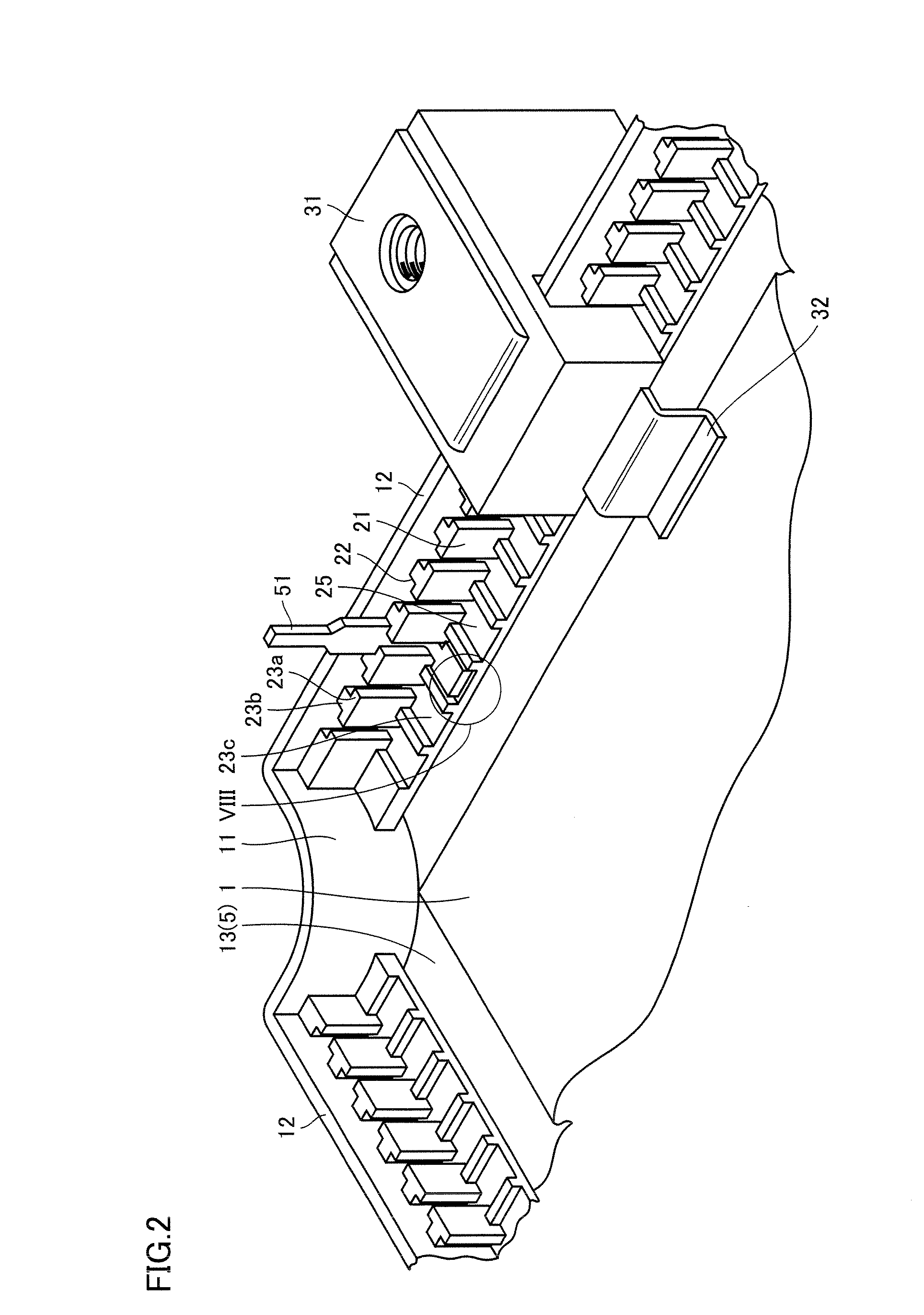
[0037]Referring to FIGS. 1 and 2, a power semiconductor package identified as the semiconductor device according to the present embodiment includes a base board 5, a semiconductor mounting substrate (insulating substrate) 1 rested thereon, a mother case 11 fixedly attached to base board 5 and serving as an enclosure, a securing member 21, and a screw terminal 31 and a pin terminal 51 as the terminals. Base board 5 is made of a material exhibiting excellent heat radiation, such as copper, copper alloy or the like, and semiconductor mounting substrate 1 is rested thereon. Semiconductor mounting substrate 1 is made of an insulating substrate of ceramic or the like, and a wiring pattern of copper foil or copper plate is formed on its surface, with a power semiconductor element and the like being fixedly attached on the wiring pattern. Mother case 11 is in an approximately rectangular shape, and has an opening 13. Semiconductor mounting substrate 1 is accommodated inside opening 13, as m...

second embodiment

[0062]Referring to FIGS. 14 and 15, the screw terminal 31 of the present embodiment differs from the screw terminal shown in FIG. 4 in that the electrode 32 has a plurality of strips.

[0063]Electrode 32 formed with slits has three strips each having a tip end portion 37, with two projections 38 formed between the respective three strips. Screw terminal main body 35 has an opening 39 formed between its rectangular parallelepiped portion and overhanging portion 35a, and projections 38 branch off from electrode 32 downward to penetrate through opening 39. Projections 38 are formed by preparing a metal plate having a rectangular shape, making four cuts in the metal plate in the longitudinal direction from its tip end portion 37, and by bending the split portions. The remaining portions (strips) other than those constituting projections 38 are bent at positions different from projections 38, and their tip end portions 37 serving as electrodes contact semiconductor mounting substrate 1 (FI...

third embodiment

[0066]Referring to FIGS. 16 and 17, the screw terminal 31 of the present embodiment differs from the screw terminal of the second embodiment in that a tip end 38a of projection 38 is connected to electrode 32. Projection 38 branches off from electrode 32 downward to penetrate through opening 39 between the rectangular parallelepiped portion and overhanging portion 35a of screw terminal main body 35, and then extends in a horizontal direction so that its tip end 38a is connected to electrode 32.

[0067]Otherwise, the structure of screw terminal 31 is identical to that of the screw terminal shown in FIGS. 14 and 15, and therefore, the same members have the same reference characters allotted, and description thereof will not be repeated.

[0068]In the power semiconductor package of the present embodiment, tip end 38a of projection 38 is connected to electrode 32. As such, a current can be supplied to projection 38 as well, and thus, a large current can be supplied to screw terminal 31.


PUM


Abstract

The power semiconductor package includes a semiconductor mounting substrate, a mother case having an opening and containing the semiconductor mounting substrate therein, a securing member having a plurality of securing positions formed along a rim constituting the opening, and a screw terminal and a pin terminal secured at the rim and electrically connected to the semiconductor mounting substrate. The screw terminal and the pin terminal are each secured by the securing member at one of the plurality of securing positions thereof. Thus, the package can adapt to variation in shape and arrangement of terminals due to differences in circuit configuration and the like of the semiconductor apparatuses, and can reduce restriction on the layout within the enclosure.

Description

BACKGROUND OF THE INVENTION[0001]1. Field of the Invention[0002]The present invention relates to a semiconductor device having terminals, and more particularly to a semiconductor device having terminals that can adapt to variation in arrangement of pin and screw terminals serving as electrodes.[0003]2. Description of the Background Art[0004]Power semiconductor packages for semiconductor apparatuses used for inverter drive of industrial equipment and the like have various configurations such as CIB, 7 in 1, 6 in 1, and 2 in 1. CIB refers to a package incorporating a converter, six inverters, and a brake. 7 in 1 refers to a package incorporating six inverters and a brake. 6 in 1 refers to a package incorporating six inverters, and 2 in 1 refers to a package incorporating two inverters.[0005]In these power semiconductor packages, terminals differ in shape and arrangement from each other, due to differences in internal circuit, rating and specification of the semiconductor apparatuses f...

Claims


Application Information

Patent Timeline
IPC IPC(8): H01L23/48
CPCH01R11/26H05K7/1432H01L2924/0002H01L2924/00
Inventor MATSUMOTO, MASAFUMI
Owner MITSUBISHI ELECTRIC CORP
Learn More