Organic electro-luminescence display device and method for fabricating the same

a technology of which is applied in the manufacture of electric discharge tube/lamp, discharge tube luminescnet screen, electrode system, etc., can solve the problems of reducing the lifetime reducing the reliability and reducing the emitted layer of the organic electro-luminescence display device. the effect of reliability and the increase of the lifetim

Active Publication Date: 2008-01-03
LG DISPLAY CO LTD
View PDF15 Cites 23 Cited by
  • Summary
  • Abstract
  • Description
  • Claims
  • Application Information

AI Technical Summary

Benefits of technology

[0010] An object of the present invention is to provide an organic electro-luminescence display device that can effectively block...

Problems solved by technology

Meanwhile, an organic emission layer of a conventional organic electro-luminescence display device is susceptible to moisture and oxygen.
The occurrence of the dark spots will reduce the li...

Method used


Image

  • Organic electro-luminescence display device and method for fabricating the same
  • Organic electro-luminescence display device and method for fabricating the same
  • Organic electro-luminescence display device and method for fabricating the same

Examples


first embodiment

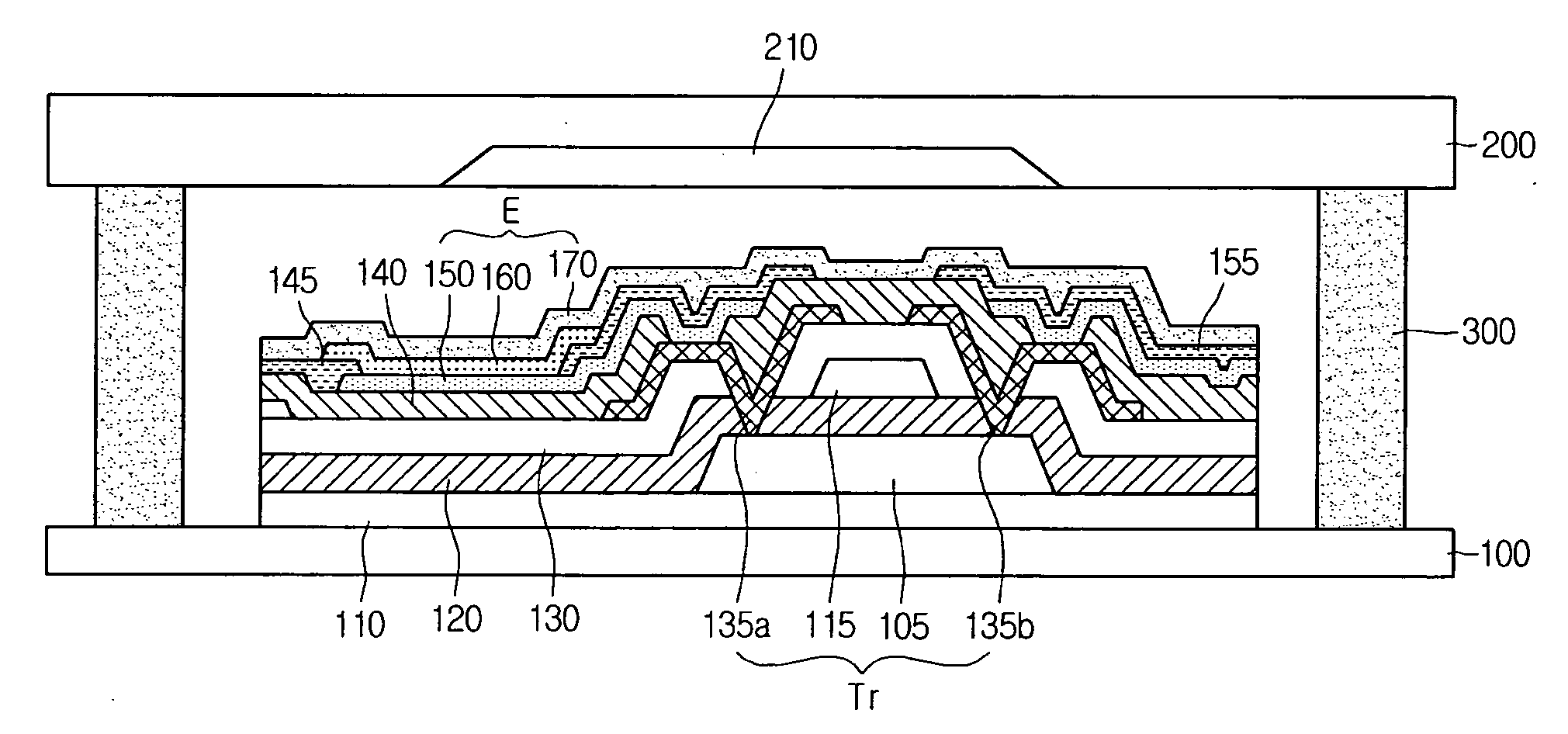
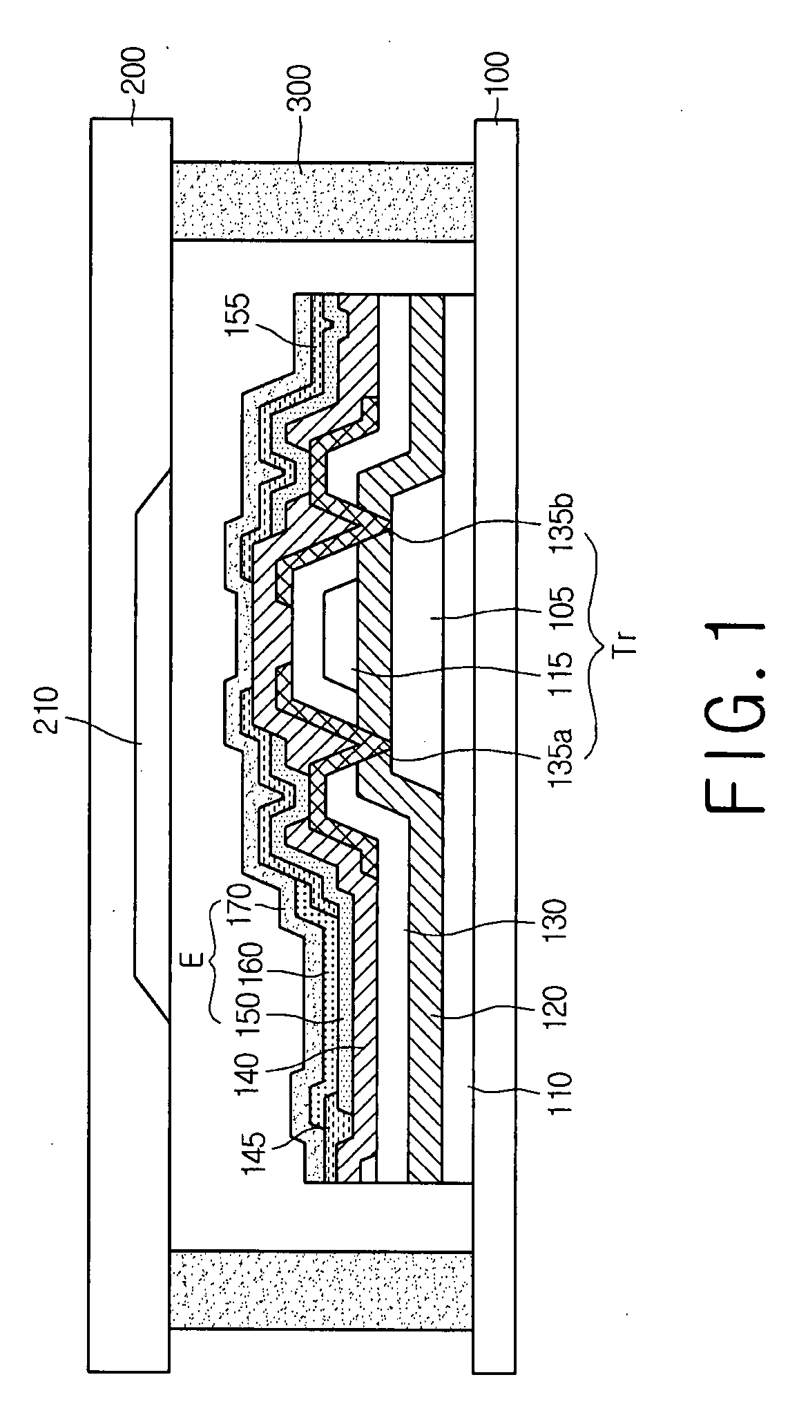
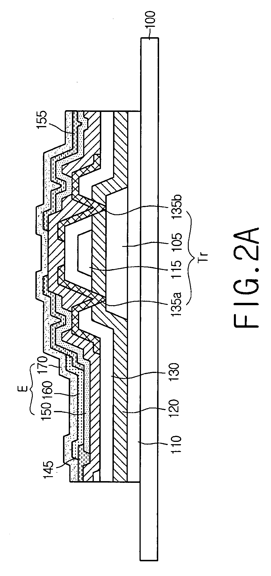
[0022]FIG. 1 is a cross-sectional view of an organic electro-luminescence display device according to the present invention.

[0023] Referring to FIG. 1, an organic electro-luminescence display device according to a first embodiment of the present invention includes a first substrate 100 and a second substrate 200.

[0024] A TFT Tr and an organic electro-luminescent diode E are formed on a first substrate 100. The organic electro-luminescent diode E is electrically connected to the TFT Tr.

[0025] A buffer layer 110 is formed on the first substrate 100. A semiconductor layer 105 is formed on the buffer layer 110. The semiconductor layer 105 may be formed of polysilicon. A gate insulating layer 120 is formed over the first substrate 100 on which the semiconductor layer 105 is formed. A gate electrode 115 is formed above a portion of the gate insulating layer 110 corresponding to the semiconductor layer 105.

[0026] A source region and a drain region are defined in the semiconductor layer ...

second embodiment

[0063]FIG. 3 is a cross-sectional view of an organic electro-luminescence display device according to the present invention. Since the organic electro-luminescence display device of FIG. 3 is similar to that of FIG. 1, except that a TFT and an organic electro-luminescent diode E are formed in the different substrates, a duplicate description will be omitted for conciseness.

[0064] Referring to FIG. 3, the organic electro-luminescence display device according to the second embodiment of the present invention includes first and second substrates 400 and 500 spaced apart from each other by a predetermined distance and attached to each other by a sealant 600. A TFT Tr is formed on the first substrate 400, and an organic electro-luminescent diode E is formed on the second substrate 500.

[0065] Since it is difficult to separately form a moisture absorbent in such a dual panel type organic electro-luminescence display device, an encapsulation process of attaching the first substrate 400 to ...


PUM


Abstract

An organic electro-luminescence display device and a method for fabricating the same are provided. A first substrate and a second substrate are sealed by a sealant. An organic electro-luminescent diode is formed on the first substrate. The sealant contains a frit glass and a light-heat converter. The frit glass can reduce the moisture and oxygen transmission rate by preventing the organic electro-luminescent diode from being thermally decomposed during a curing process. Since the two substrates are encapsulated by the frit glass, the lifetime and reliability of the organic electro-luminescence display device can be increased.

Description

[0001] This application claims the benefit of Korean Patent Application No. 2006-0061211, filed on Jun. 30, 2006, which is hereby incorporated by reference as if fully set forth herein. BACKGROUND OF THE INVENTION [0002] 1. Field of the Invention [0003][0004] The present invention relates to an organic electro-luminescence display device, and more particularly, to an organic electro-luminescence display device having an improved reliability and an extended lifetime, and a method for fabricating the same. [0005] 2. Description of the Related Art [0006] Organic electro-luminescence display devices display an image using light generated by the recombination of electrons and holes in an organic emission layer. Unlike liquid crystal display devices (LCDs), the organic electro-luminescence display devices require no backlight assembly because they display an image using light generated from the organic emission layer. Therefore, the organic electro-luminescence display devices are lightwe...

Claims


Application Information

Patent Timeline
IPC IPC(8): H01L51/52H01L51/56
CPCH01L27/3251H01L51/5259H01L51/5246H10K59/127H10K59/874H10K59/8722H05B33/04H10K50/8426H10K50/846
Inventor KIM, JEONG HYUNYOO, CHOONG KEUNCHO, HEUNG LYULLEE, JOON SUKMOON, JONG SEOKYOO, IN SUN
Owner LG DISPLAY CO LTD
Why Eureka
Try Eureka