Semiconductor Devices Including Impurity Doped Region and Methods of Forming the Same

Inactive Publication Date: 2008-01-10
SAMSUNG ELECTRONICS CO LTD
View PDF5 Cites 6 Cited by
  • Summary
  • Abstract
  • Description
  • Claims
  • Application Information

AI Technical Summary

Benefits of technology

[0014] Exemplary embodiments of the present invention also provide a semiconductor device including an impurity doped region having an excellent electrical property and a small junction depth and a method of forming the same.

Problems solved by technology

Accordingly, the junction depth of the impurity doped region may increase and the semiconductor device may degrade despite the RTA process.
This excess of inactivated dopant may lead to detects such as vacancy and / or dislocation in a surface of the impurity doped region.

Method used


Image

  • Semiconductor Devices Including Impurity Doped Region and Methods of Forming the Same
  • Semiconductor Devices Including Impurity Doped Region and Methods of Forming the Same
  • Semiconductor Devices Including Impurity Doped Region and Methods of Forming the Same

Examples


Embodiment Construction

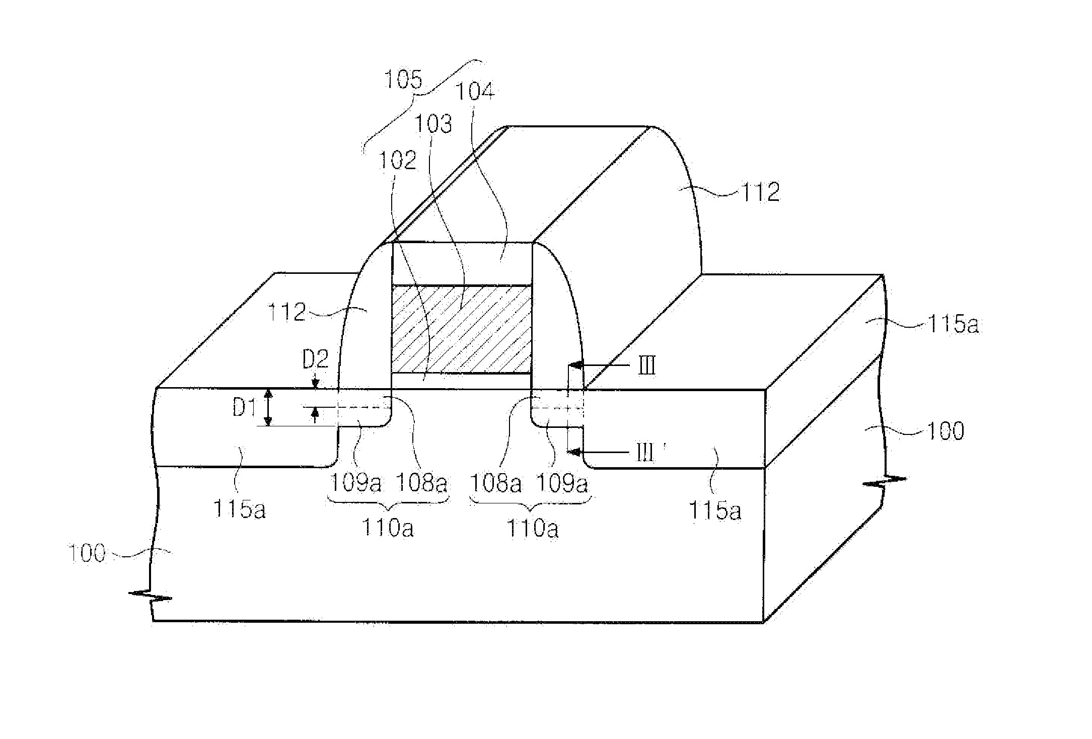
[0028] Exemplary embodiments of the present invention will be described below in more detail with reference to the accompanying drawings. The present invention may, however, be embodiment in different forms and should not be constructed as limited to the exemplary embodiments set forth herein. In the figures, the dimensions of layers and regions may be exaggerated for clarity of illustration. Like reference numerals may refer to like elements throughout.

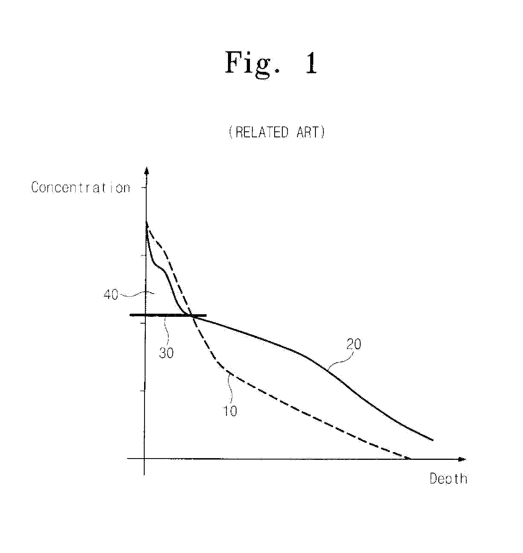
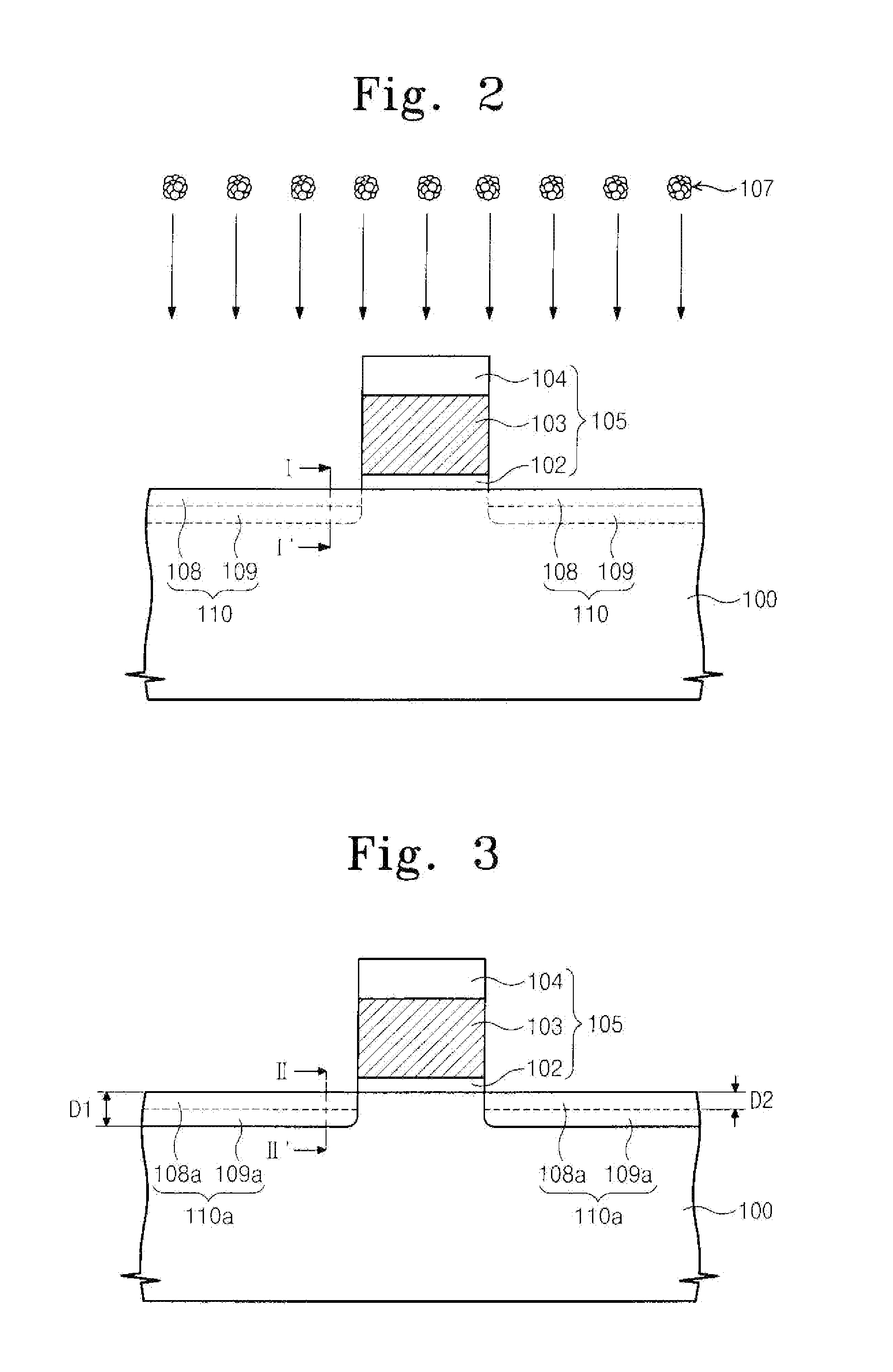
[0029]FIGS. 2 and 3 are sectional views illustrating a method of forming a semiconductor device including an impurity doped region according to an exemplary embodiment of the present invention. FIG. illustrates the dopant concentration as a result of the depth of the impurity doped region taken along a line I-I′ of FIG. 2. FIG. 5 illustrates the dopant concentration as a result of the depth of the impurity doped region taken along a line II-II′ of FIG. 3. FIG. 6 is a flowchart illustrating a method of forming an impurity doped regio...


PUM


Abstract

A semiconductor device including an impurity doped region and a method of forming the same. The method includes implanting cluster-shaped dopant ions into a semiconductor substrate to form an impurity implantation region. An annealing process is performed on the impurity implantation region to form an impurity doped region.

Description

CROSS-REFERENCE TO RELATED APPLICATIONS [0001] This application claims priority under 35 U.S.C § 119 to Korean Patent Application No. 10-2006-0009775, filed on Feb. 1, 2006, the entire contents of which are hereby incorporated by reference. BACKGROUND OF THE INVENTION [0002] 1. Technical Field [0003] The present disclosure relates to semiconductor devices and methods of forming the same, and more particularly, to semiconductor devices including an impurity doped region and methods of forming the same. [0004] 2. Discussion of the Related Art [0005] Semiconductor devices may include a semiconductor substrate having regions that are doped with impurities. Impurities may be either p-type dopants or n-type dopants. The impurity doped regions may conduct electricity in a desired manner. Impurity doped regions are generally used as source / drain regions of a MOS (metal oxide semiconductor) field effect transistor (hereinafter, referred to as a transistor). Generally an impurity doped region...

Claims


Application Information

Patent Timeline
IPC IPC(8): H01L29/78H01L21/265H01L21/336
CPCH01L21/26513H01L21/26566H01L29/6659H01L29/7833F24F7/08F24F13/30H01L21/2658
Inventor UENO, TETSUJIRHEE, HWA-SUNGLEE, HO
Owner SAMSUNG ELECTRONICS CO LTD
Why Eureka
Try Eureka