Semiconductor Device, Method of Manufacturing A Semiconductor Device, and Display Device

Inactive Publication Date: 2012-05-17
TOHOKU UNIV
View PDF5 Cites 14 Cited by
  • Summary
  • Abstract
  • Description
  • Claims
  • Application Information

AI Technical Summary

Benefits of technology

[0051]According to this invention, by providing a patterned Al or Al alloy gate electrode with an anodic oxide film attached thereto as a gate insulating film, using a non-aqueous solution and by burying a region around the gate insulating film with an insulating film and flattening it, it is possible to solve various problems which arise when a gate electrode is formed in a groove after the groove is formed on an insulator. Thus, it is possible to achieve high carrier mobility with the flat and thin gate insulating film. Further, using an Al—Zr—Ce alloy or an Al—Mg—Zr—Ce alloy as a gate electrode and using, as a gate insulating film, an anodic oxide film obtained by anodizing a surface of the gate electrode using a non-aqueous solution, it is possible to provide an insulated gate transistor having very high carrier mobility due to the gate insulating film which is thin and excellent in electrical properties.

Problems solved by technology

Further, when increasing the size of the display device, since the wiring pattern itself becomes longer, it is necessary to reduce the electrical resistance of the wiring pattern.

Method used


Image

  • Semiconductor Device, Method of Manufacturing A Semiconductor Device, and Display Device
  • Semiconductor Device, Method of Manufacturing A Semiconductor Device, and Display Device
  • Semiconductor Device, Method of Manufacturing A Semiconductor Device, and Display Device

Examples


first embodiment

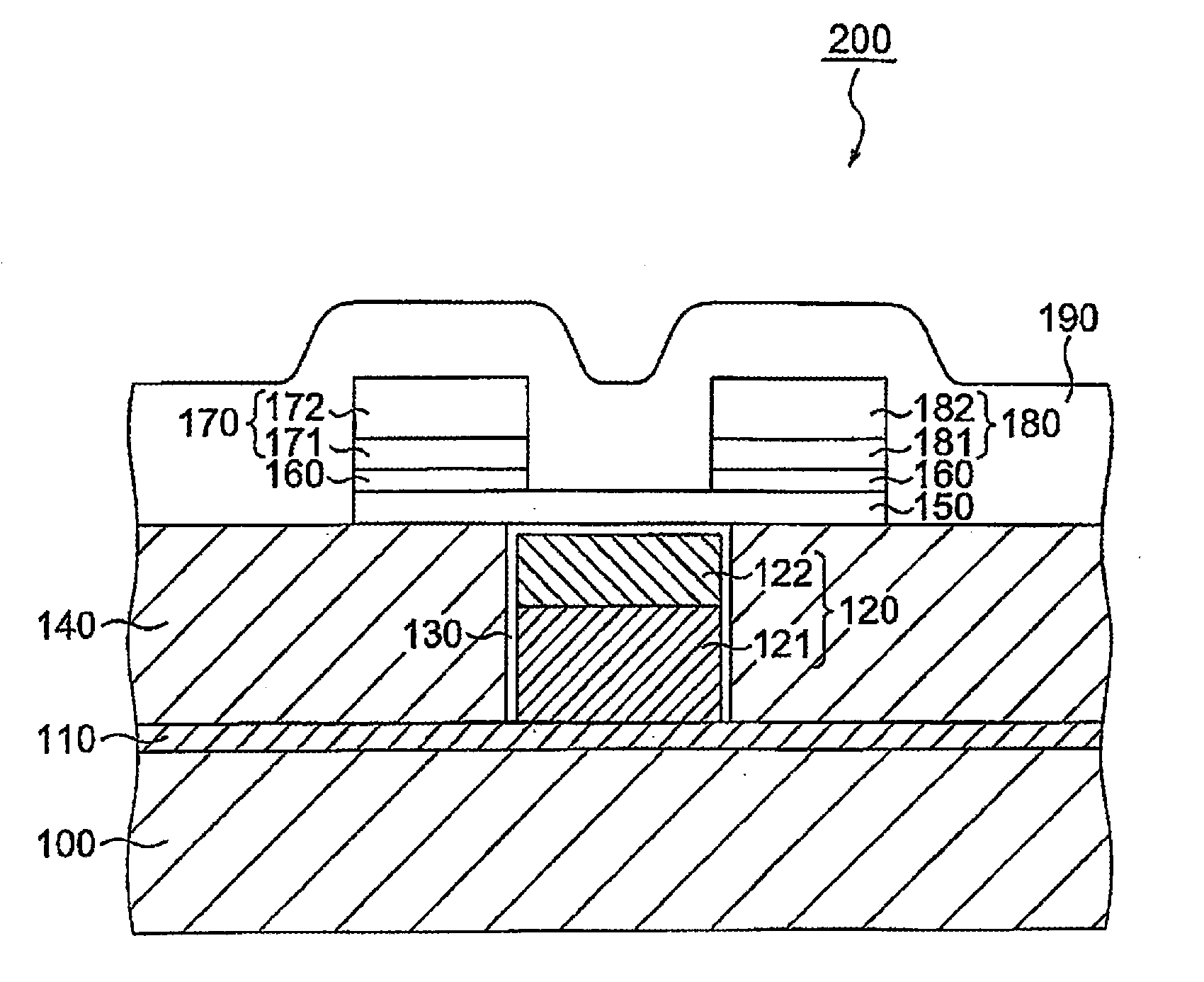
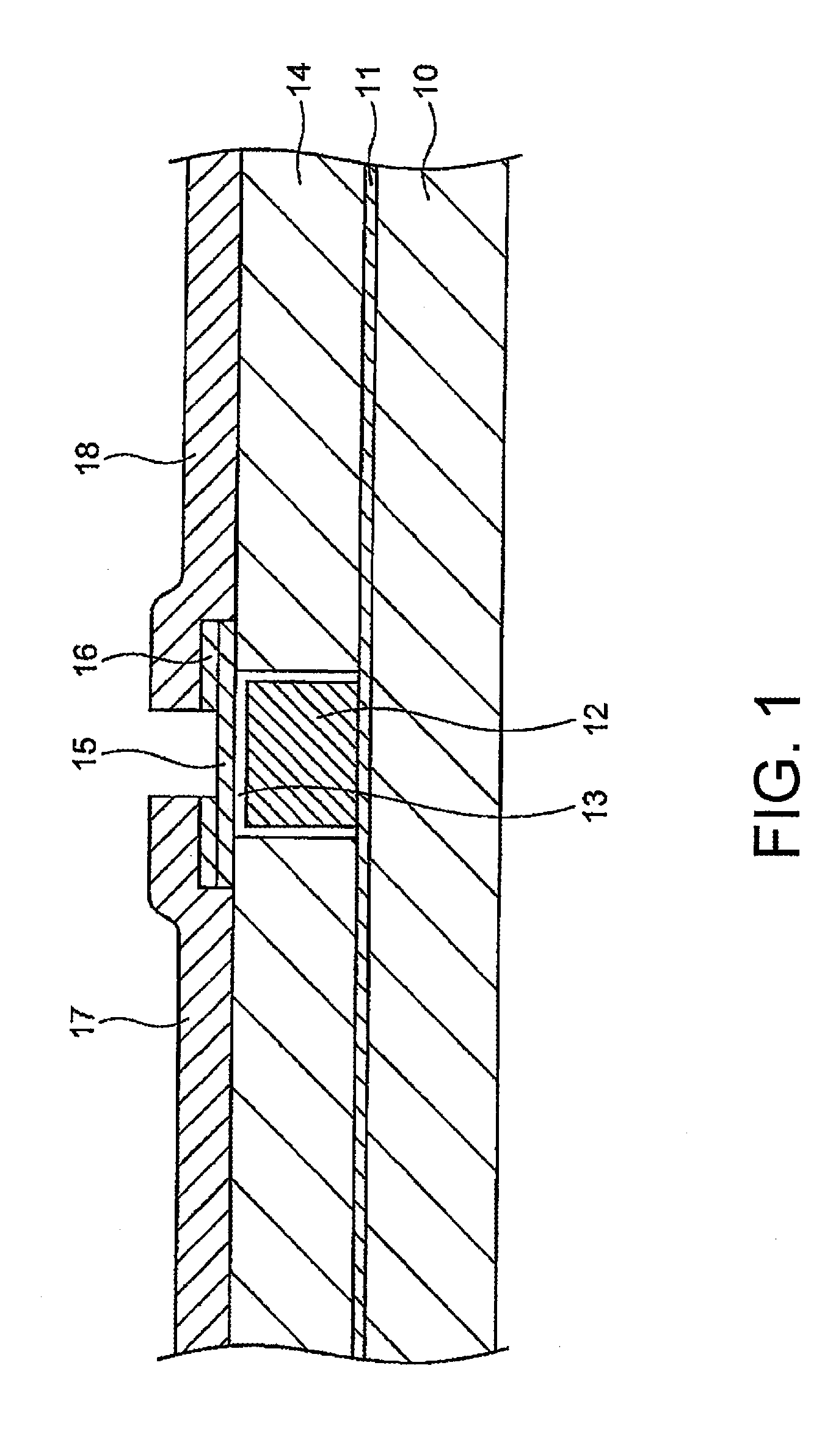
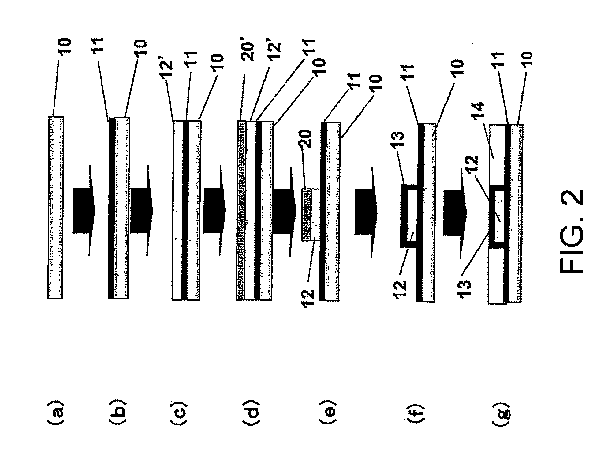
[0058]FIG. 1 is a cross-sectional view showing an example of the structure of a thin film transistor (TFT) of this invention. The thin film transistor comprises a Na-diffusion preventing film 11 formed on a glass substrate (insulating substrate) 10, a gate electrode / wiring layer 12 (gate electrode portion is shown in the figure) of Al or an Al alloy formed in a predetermined pattern on the Na-diffusion preventing film 11, a dense anodic oxide film 13 formed on surfaces of the gate electrode 12 by anodization using a non-aqueous solution, a transparent resin layer 14 formed around the gate electrode / wiring layer 12 to approximately the same height as the gate electrode 12 and its upper-surface anodic oxide film 13 so as to be substantially flush with the upper-surface anodic oxide film 13, a semiconductor layer 15 formed over the gate electrode 1 through the gate insulating film 13, and a source electrode 17 and a drain electrode18 respectively connected to electrode connection regio...


PUM


Abstract

A semiconductor device comprises a gate electrode that is provided on a substrate and contains Al or an Al alloy; a gate insulating film that is so formed as to cover at least the upper surface of the gate electrode and contains an anodic oxide film that is obtained by anodizing the Al or Al alloy of the gate electrode; and an insulator layer that is so formed on the substrate as to surround the gate electrode and has a thickness that is substantially equal to a total of the thickness of the gate electrode and the thickness of the gate insulating film formed on the upper surface of the gate electrode.

Description

TECHNICAL FIELD[0001]This invention relates to a semiconductor device, particularly a thin film transistor (TFT), and further relates to a manufacturing method thereof.BACKGROUND ART[0002]Generally, a display device, such as a liquid crystal display device, an organic EL device, or an inorganic EL device is fabricated by successively forming and patterning films into conductive patterns such as a wiring pattern and an electrode pattern on a substrate having a flat main surface. Thus, the display device is manufactured by successively forming and patterning an electrode film, various films necessary for elements that constitute the display device, and so on.[0003]In recent years, there is a growing demand for an increase in size with respect to this type of display device. In order to form a large-size display device, it is necessary to form more display elements on a substrate with high accuracy and to electrically connect these elements to a wiring pattern. In this case, insulating...

Claims


Application Information

Patent Timeline
IPC IPC(8): H01L33/08H01L21/28H01L23/48H01L29/786
CPCG02F1/1368H01L21/02178H01L2924/0002H01L21/02194H01L21/02244H01L21/28008H01L23/53219H01L27/1248H01L29/42384H01L29/458H01L29/4908H01L29/66765H01L29/78636H01L2924/12044H01L2924/00H01L29/51
Inventor OHMI
Owner TOHOKU UNIV
Why Eureka
Try Eureka