Method of forming probe card assembly

a technology of probe tip and assembly method, which is applied in the direction of manufacturing tools, semiconductor/solid-state device testing/measurement, instruments, etc., can solve the problems of non-planarity of the probe tip, z error in the manufacturing process, and usually direct errors, etc., to achieve easy assembly and disassembly, and less expensive construction. , the effect of high mechanical precision of the substrate location

Active Publication Date: 2008-01-10
FORMFACTOR INC
View PDF15 Cites 9 Cited by
  • Summary
  • Abstract
  • Description
  • Claims
  • Application Information

AI Technical Summary

Benefits of technology

[0015] An embodiment of the current invention provides for a new class of probe card assembly that is not a FPCA or an APCA. Instead of relying on shims or other similar means to achieve initial parallelism in the assembly process, it provides for a mechanism to align a probe-bearing substrate into parallel position and semi-permanently lock it into that position. Because of the locking mechanism, the substrate position and orientation is not adjusted once it is mounted in position. An advantage of a semi-permanent locking mount is that it is mechanically and thermally stable relative to an adjustable mount. Also, the semi-permanent mount is less expensive to build.
[0016] The semi-permanent mount has the characteristics of being easily assembled and disassembled in case service or repair of the probe card is necessary. Some parts of the mounting mechanism may be single-use and need replacement each time the probe card is re-assembled.
[0017] Another embodiment of the current invention provides for a semi-permanent, aligned but non-adjustable mount of a plurality of probe substrates to a superstructure. The alignment method disclosed provides for extremely high mechanical precision of substrate location without the cost, complexity and size of a fully-adjustable mechanical mount per substrate.

Problems solved by technology

In practice, there is some manufacturing process-related z error (non-planarity of the probe tips) caused by film stresses, etch control, assembly control, etc. as well as systemic z errors caused by a warping or curving in the surface of the probe contactor substrate.
Some errors are most directly related to the fabrication of the probes on the probe contactor substrate rather than the probe card assembly design.
However, some errors are usually directly related to the probe card assembly and the way the PCB is mounted with the probe contactor substrate or substrates.
However, the machining tolerances required for parallelism, particularly in the case of large area probe cards, can be difficult to achieve.
Shimming, though a practical alternative, is difficult to perform accurately in a manufacturing environment to the tolerances required (on the order of microns).
It is also common practice in the art to mount the probe card and lap the probe tips parallel to the mount, though this technique introduces unwanted damage to the probe tips and is not practical for coated probes (probes with a thin coating of material that is different from the base spring material).
However adjustability also has a number of significant disadvantages including drift of the adjustment over time and thermal cycling, cost of the relatively complex precision mechanical assemblies required and difficulty of assembly.
Furthermore, the adjustment mechanism can take significant space and limit the density of adjacent blocks of probes.
This particular design is particularly expensive, difficult to assemble, and complex.
In addition, the large number of mechanical components required to achieve adjustability make the design inherently thermally unstable.
The trouble with this method is that the mount is relatively large (so that it does not fit in the conventional envelope provided for probe cards) cumbersome, expensive and unstable (i.e. drifts in position as a function of time, particularly when exposed to thermal excursions).

Method used


Image

  • Method of forming probe card assembly
  • Method of forming probe card assembly
  • Method of forming probe card assembly

Examples


Embodiment Construction

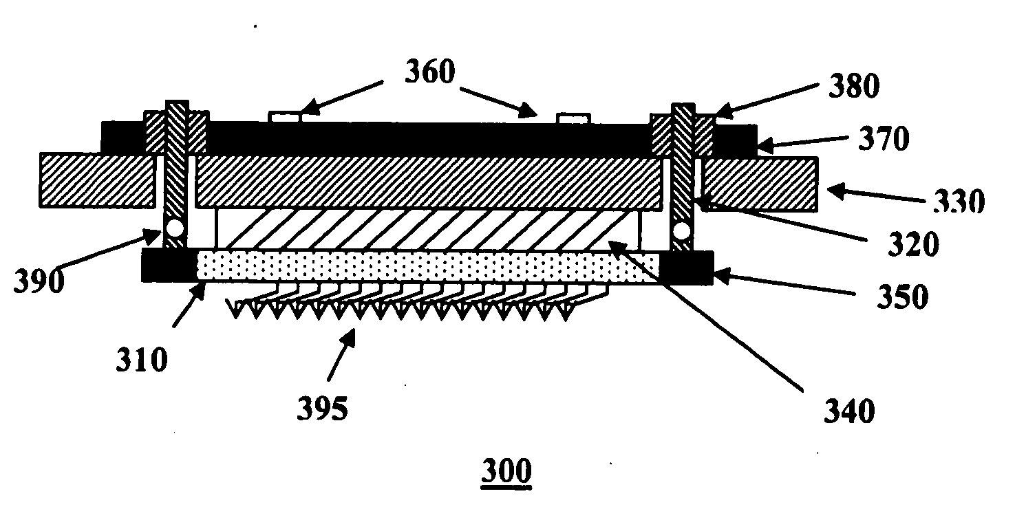
[0041]FIG. 3 illustrates a probe card assembly 300 having a semi-permanent mount according to an embodiment of the present invention. As shown in FIG. 3, the probe card assembly is comprised of a probe contactor substrate 310 having support structures, illustrated as support posts 320, coupled thereto. The probe contactor substrate 310 is assembled so as to be coupled to the printed circuit board (“PCB”) 330 with a compliant interposer 340 in place. The contactor substrate 310 is aligned with the reference points 360 in an orientation such that the probe contactors' 395 tips are in a plane that is parallel to plane formed by the reference points 360. The reference points 360 in FIG. 3 are of the kinematic mountings points variety as discussed earlier, however, it is important to note that if the probe card assembly does not have such mounting points 360, then the probe contactors' 395 tips are in a plane that is parallel to another reference plane such as that of the bottom surface ...


PUM

PropertyMeasurementUnit
heightaaaaaaaaaa
temperatureaaaaaaaaaa

Abstract

A probe card assembly has a probe contactor substrate having a plurality of probe contactor tips thereon and a probe card wiring board with an interposer disposed between the two. Support posts contacting the probe contactor substrate are vertically adjustable until secured by a locking mechanism which is coupled to the probe card wiring board. When the posts are secured in a fixed position, the position is one in which the plane of the plurality of probe contactor substrates is substantially parallel to a predetermined reference plane.

Description

BACKGROUND OF THE INVENTION [0001] 1. Field of the Invention [0002] Embodiments of the present invention are directed to a probe card assembly and more particularly to a method and apparatus for providing a probe card assembly with a precisely fixed probe substrate position relative to the reference plane of the probe card. [0003] 2. Description of Related Art [0004] A modern probe card assembly used to test wafers of semiconductor chips generally consists of a Printed Circuit Board (PCB) (also referred to as a printed wiring board or probe card wiring board), a probe contactor substrate having probes for contacting the wafer (sometimes referred as a probe head), and an interposer connecting the PCB to the probe contactor substrate. [0005] Probes (also referred to as probe contactors) are generally compliant mechanisms including at least one spring which have some limited range of compliance in a vertical direction (the “z” direction). Some probes have minimal or no compliance. When...

Claims


Application Information

Patent Timeline
Patent Type & Authority Applications(United States)
IPC IPC(8): G01R1/073H01R43/00
CPCG01R1/07378Y10T29/53243G01R3/00G01R1/073H01L22/00
Inventor GARABEDIAN, RAFFITEA, NIM HAKWANG, STEVENKARKLIN, HEATHER
Owner FORMFACTOR INC
Why Eureka
Try Eureka