Sequential circuit design for radiation hardened multiple voltage integrated circuits

a technology of integrated circuits and circuits, applied in the field of circuit design, can solve the problems of increasing the setup of master and slave latches, increasing the power consumption of the overall circuit, and increasing the risk of ionizing radiation exposure of space-based circuits, so as to achieve superior radiation hardening characteristics, reduce power consumption, and reduce the effect of power consumption

Active Publication Date: 2008-01-10
STC UNM
View PDF4 Cites 13 Cited by
  • Summary
  • Abstract
  • Description
  • Claims
  • Application Information

AI Technical Summary

Benefits of technology

[0012]Accordingly, the present invention includes a circuit that is adapted for low power consumption and radiation hardness. In its various embodiments described below, the circuit includes a master latch connected to an input and a slave latch connected to the master latch. The master latch and the slave latch each further include one or more logic gates adapted to be substantially maintained at a high voltage. The circuit described herein also includes a clock element connected to the master latch, the slave latch, and a power source, wherein the clock element adapted to cause the master latch to transition between a first state and a second state. The power source can be adapte

Problems solved by technology

However, as die size and integration have increased, overall power consumption has risen dramatically.
Unlike most terrestrial applications, however, space-based circuits are much more likely to be exposed to ionizing radiation, such as from a heavy ion or proton.
Ionizing radiation can cause single event upsets (SEU), which introduce undesirable current into the IC.
Unfortunately, however, the int

Method used


Image

  • Sequential circuit design for radiation hardened multiple voltage integrated circuits
  • Sequential circuit design for radiation hardened multiple voltage integrated circuits
  • Sequential circuit design for radiation hardened multiple voltage integrated circuits

Examples


Embodiment Construction

[0025]The following description of the preferred embodiments is provided to enable any person skilled in the art to make or use the present invention. Various modifications to these embodiments will be readily apparent to those skilled in the art, and the generic principles defined herein may be applied to other embodiments without departing from the spirit or scope of the invention as set forth in the appended claims.

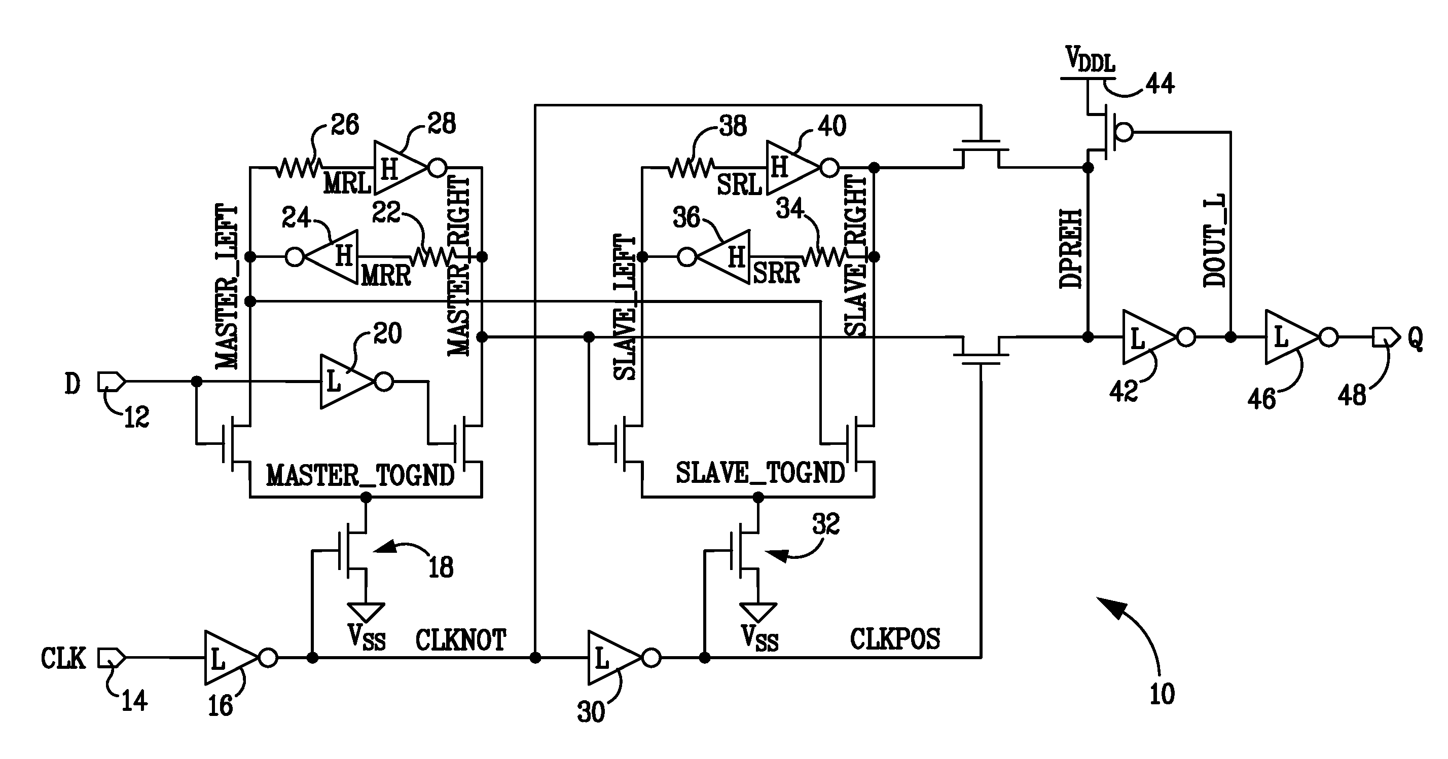
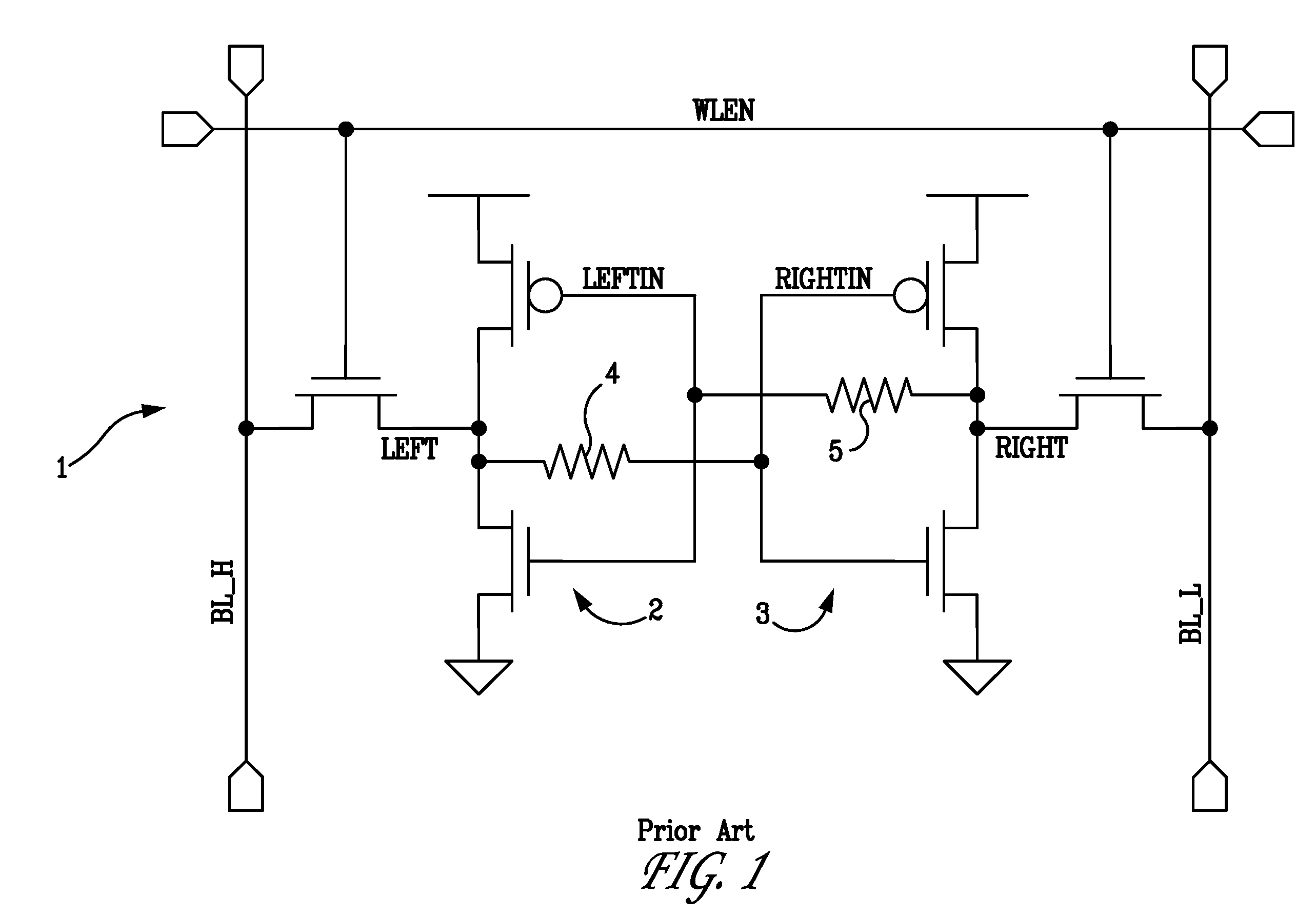
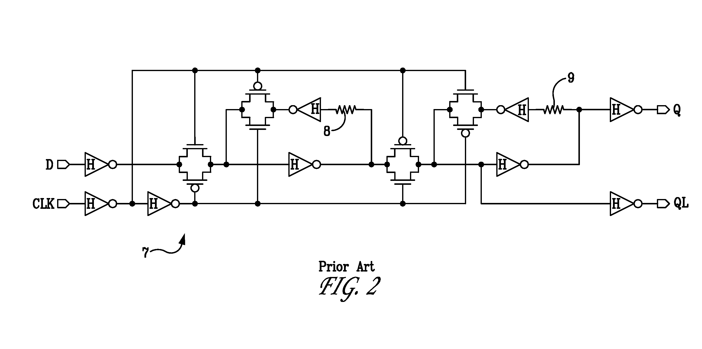
[0026]The present invention includes a radiation hardened sequential circuit, such as a bistable circuit, flip-flop or other suitable design that presents substantial immunity to SEU, SEE and SET while maintaining a low operating voltage. As such, the circuit of the present invention is particularly well-suited for certain applications in which radiation hardness and low power consumption are desirable, such as for example, circuitry for use in aerospace and / or satellite devices and / or systems.

[0027]The circuit of the preferred embodiment includes a master latch connec...


PUM


Abstract

The present invention includes a radiation hardened sequential circuit, such as a bistable circuit, flip-flop or other suitable design that presents substantial immunity to ionizing radiation while simultaneously maintaining a low operating voltage. In one embodiment, the circuit includes a plurality of logic elements that operate on relatively low voltage, and a master and slave latches each having storage elements that operate on a relatively high voltage.

Description

CLAIM OF PRIORITY UNDER 35 U.S.C. §119[0001]The present Application for Patent claims priority to Provisional Application No. 60 / 818,821 entitled “Sequential Circuit Design for Radiation Hardened Multiple Voltage Integrated Circuits” filed Jul. 6, 2006, and assigned to the assignee hereof and hereby expressly incorporated by reference herein.CONTRACTUAL ORIGIN OF THE INVENTION[0002]The invention described herein was made with Government funding under a grant from the Sandia National Laboratories, U.S. Department of Energy, Grant No. 237095. The Government may have certain rights in this invention.BACKGROUND[0003]1. Field of the Present Invention[0004]The present invention relates generally to the field of circuit design, and more specifically to the field of integrated circuits requiring radiation hardness.[0005]2. History of the Related Art[0006]In order to minimize active power dissipation in integrated circuits (ICs), it is common for engineers to scale the power-supply voltage V...

Claims


Application Information

Patent Timeline
IPC IPC(8): H03K3/289
CPCH03K3/3562H03K3/0375
Inventor CLARK, LAWRENCE T.MCIVER, JOHN K.
Owner STC UNM
Why Eureka
Try Eureka