Method for manufacturing a magneto-resistance effect element, and magneto-resistance effect element

a technology of resistance effect and manufacturing method, which is applied in the direction of magnetic bodies, instruments, record information storage, etc., can solve the problems of severe reliability requirements of magnetic recording devices and difficult detection of minute magnetic fields

Inactive Publication Date: 2008-01-10
KK TOSHIBA
View PDF34 Cites 39 Cited by
  • Summary
  • Abstract
  • Description
  • Claims
  • Application Information

AI Technical Summary

Benefits of technology

[0046]According to the aspects of the present invention can be provided a magneto-resistance effect element which can be applied for a magnetic recording device of high density recording and develop the reliability and the method for manufacturing the same magneto-resistance effect element.

Problems solved by technology

Herein, a metal CPP-GMR element of which the spin valve film is made of a metallic layer has a smaller change in resistance to render the detection of minute magnetic field difficult.
In the future, however, the reliability of the magnetic recording device is severely required when the usage of the magnetic recording device is increased and the high density recording is also developed.

Method used


Image

  • Method for manufacturing a magneto-resistance effect element, and magneto-resistance effect element
  • Method for manufacturing a magneto-resistance effect element, and magneto-resistance effect element
  • Method for manufacturing a magneto-resistance effect element, and magneto-resistance effect element

Examples


example 1

[0199]

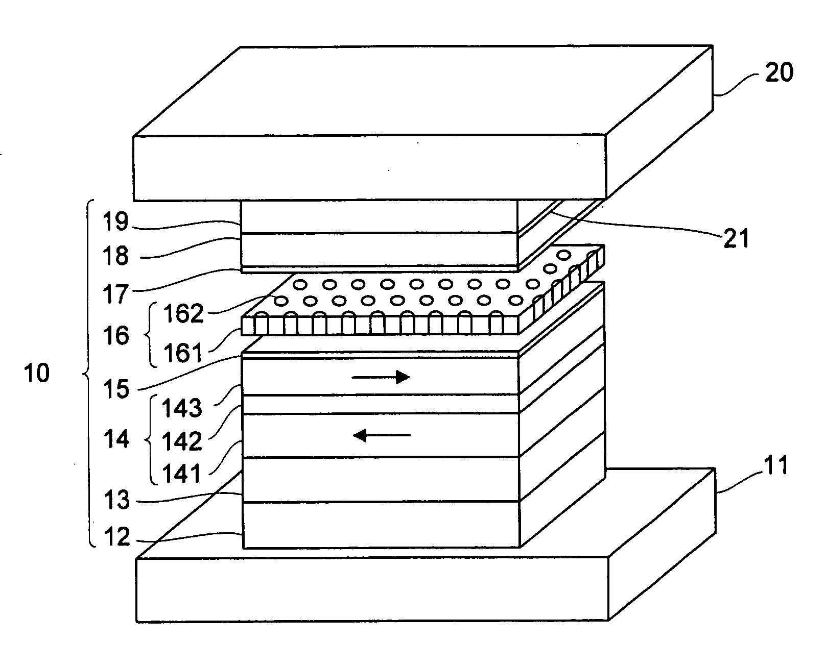
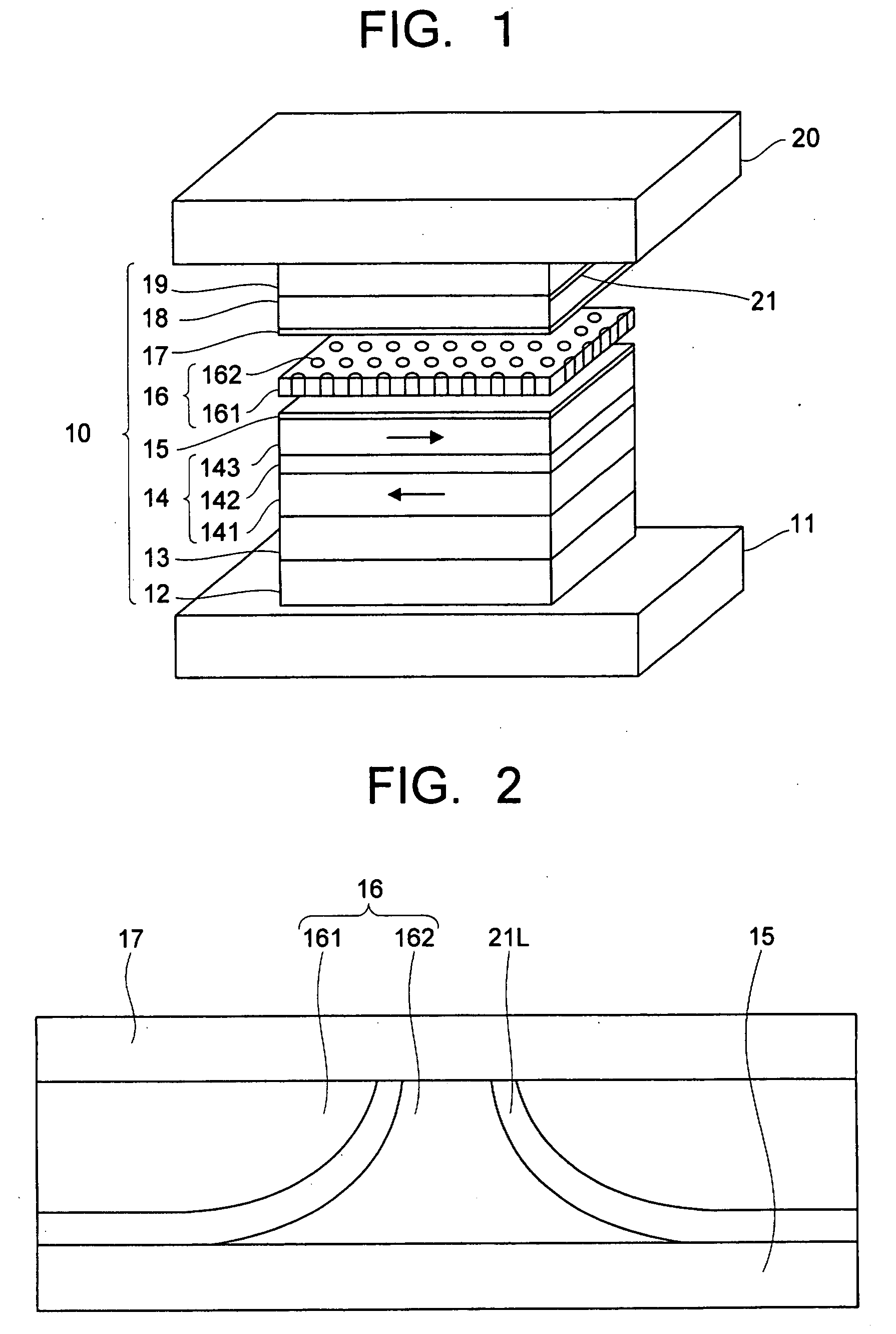
Bottom electrode 11Underlayer 12Ta 5 nm / Ru 2 nmPinning layer 13Ir22Mn78 7 nmPinned layer 14Co75Fe25 3.2 nm / Ru 0.9 nm / Fe50Co501 nm / Cu 0.25 nmx2 / Fe50Co50 1 nmMetallic layer 15Cu 0.5 nmCCP-NOL layer 16adhesion enhancing layer

composed of insulating layer 161 of Al2O3, current path 162 of Cu and Ti layer (the multilayer of Ti 0.25 nm / Al90Cu10 1 nm / Ti 0.25 nm is formed and treated by means of PIT / IAO)

Metallic layer 17Cu 0.25 nmFree layer 18Co90Fe10 1 nm / Ni83Fe17 3.5 nmCap layer 19Cu 1 nm / Ru 10 nmTop electrode 20

[0200]The manufacturing process of the CCP-NOL layer 16 will be described. The manufacturing processes of other layers can be conducted by means of conventional techniques and thus, will be omitted.

[0201]First of all, the metallic layer 15 was formed as a Cu layer with a thickness of 0.5 nm. Then, the matrix metallic layer of the adhesion enhancing layer was formed as a Ti layer with a thickness of 0.25 nm. The Ti layer constitutes the lower portion of the adhesion enhancing ...

example 2

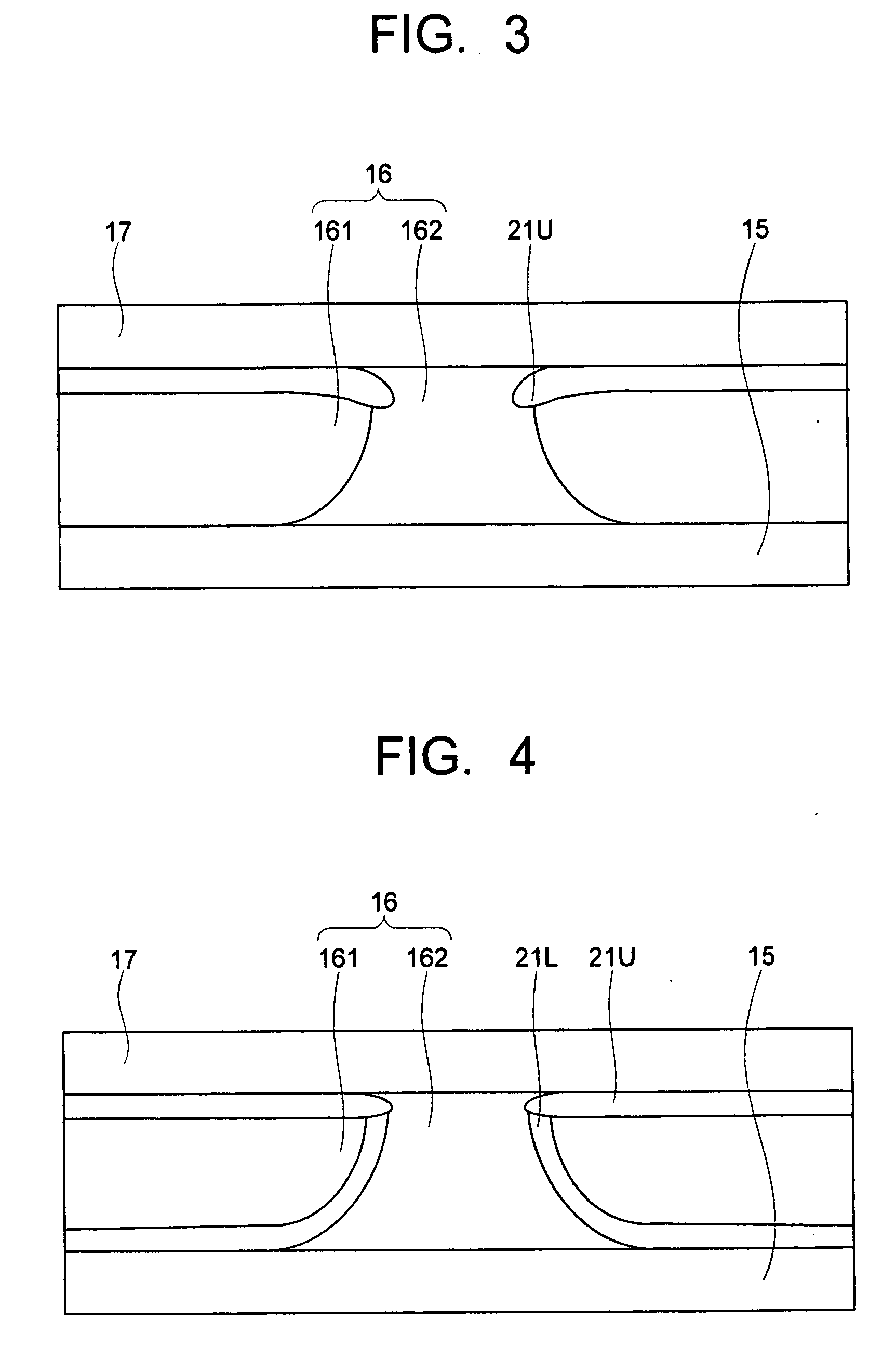
[0211]In this Example, the formation process of the adhesion enhancing layer to be formed on the insulating layer 161 was changed in comparison with Example 1. In Example 1, the matrix Ti layer of the adhesion enhancing layer is formed at the upper interface for the insulating layer 161, and then, treated by means of PIT / IAO process. In Example 2, the PIT / IAO process was conducted in advance and then, the matrix Ti layer of the adhesion enhancing layer was formed. In this case, the matrix layer of the adhesion enhancing layer can contain an element with an oxide formation energy almost equal to the oxide formation energy of the element of the insulating layer 161, in addition to the element with a lower oxide formation energy than the element of the insulating layer 161 such as Ti, Al, Si, Hf, V, W, Mg, Mo, Cr or Zr.

[0212]When the resultant magneto-resistance effect element (CCP-CPP element) 10 was observed by means of three-dimensional atomic probe, it was confirmed that the adhesi...


PUM

PropertyMeasurementUnit
thicknessaaaaaaaaaa
thicknessaaaaaaaaaa
thicknessaaaaaaaaaa

Abstract

A method for manufacturing a magneto-resistance effect element includes: forming a first magnetic layer; forming a first metallic layer, on the first magnetic layer, mainly containing an element selected from the group consisting of Cu, Au, Ag; forming a functional layer, on the first metallic layer, mainly containing an element selected from the group consisting of Si, Hf, Ti, Mo, W, Nb, Mg, Cr and Zr; forming a second metallic layer, on the functional layer, mainly containing Al; treating the second metallic layer by means of oxidizing, nitriding or oxynitiriding so as to form a current confined layer including an insulating layer and a current path with a conductor passing a current through the insulating layer; and forming, on the current confined layer, a second magnetic layer.

Description

CROSS-REFERENCE TO RELATED APPLICATIONS[0001]This application is based upon and claims the benefit of priority from the prior Japanese Patent Application No. 2006-188711, filed on Jul. 7, 2006; the entire contents of which are incorporated herein by reference.BACKGROUND OF THE INVENTION[0002]1. Field of the Invention[0003]The present invention relates to a method for manufacturing a magneto-resistance effect element which is configured such that a current is flowed in the direction perpendicular to the film surface thereof to detect the magnetization of the element and the magneto-resistance effect element.[0004]2. Description of the Related Art[0005]Recently, the miniaturization and the high density recording of a hard disk drive (HDD) is remarkably required and being progressed. In the future, it is promised to much develop the high density recording of the HDD. The HDD of high density recording can be realized by narrowing the recording track width. However, the amplitude of the ...

Claims


Application Information

Patent Timeline
Patent Type & Authority Applications(United States)
IPC IPC(8): G11B5/33G11B5/39
CPCB82Y25/00B82Y40/00G01R33/093G11B5/3906G11B5/398H01F10/3254Y10T428/1129H01F41/305H01L43/08H01L43/12H01F10/3259Y10T428/1121H01F10/3272H10N50/10H10N50/01
Inventor FUJI, YOSHIHIKOFUKUZAWA, HIDEAKIYUASA, HIROMI
Owner KK TOSHIBA
Why Eureka
Try Eureka