

Display device with suppressed occurrence of display unevenness
- Summary
- Abstract
- Description
- Claims
- Application Information
AI Technical Summary
Benefits of technology
Problems solved by technology
Method used
Image

Examples
first embodiment
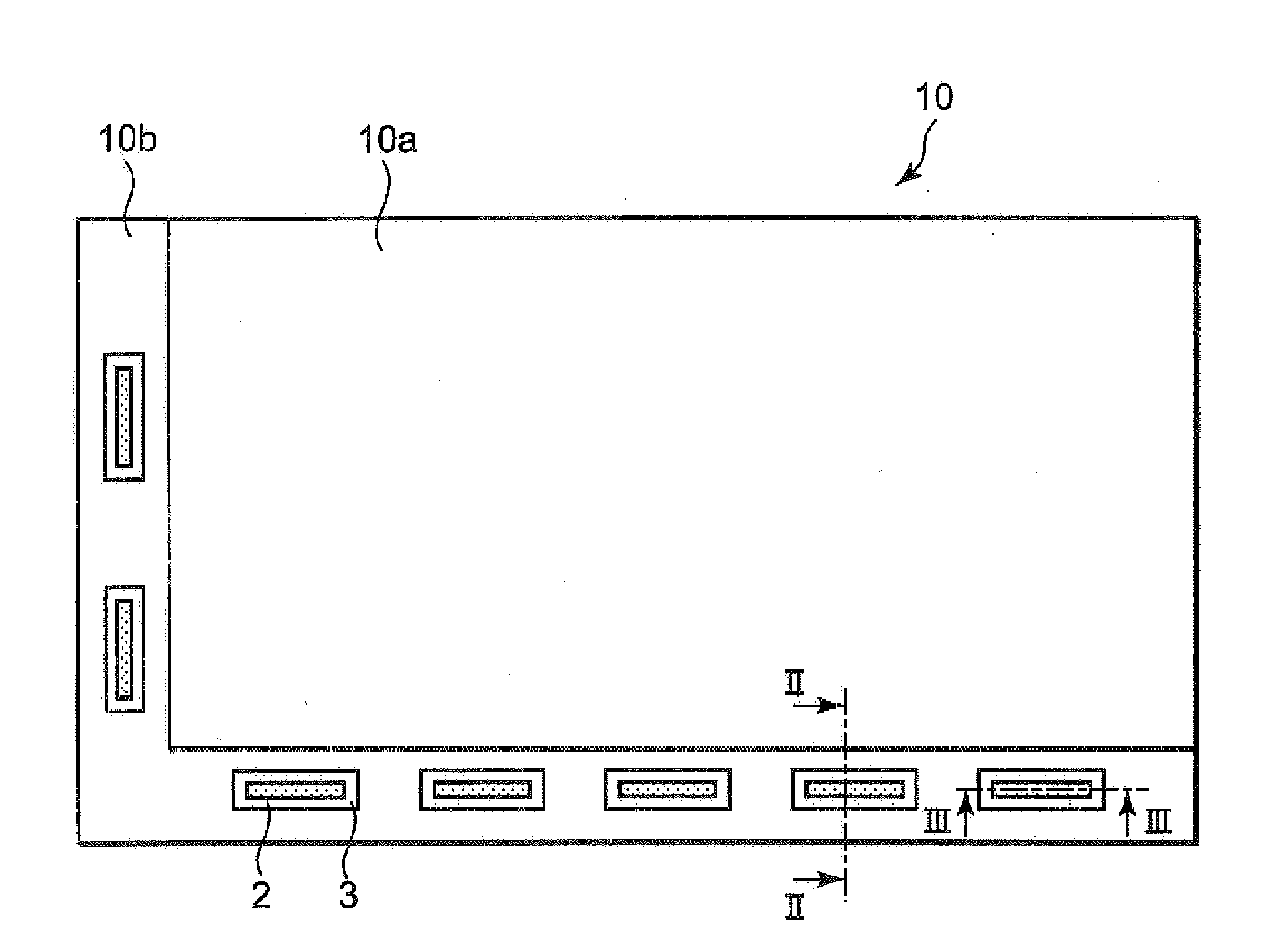
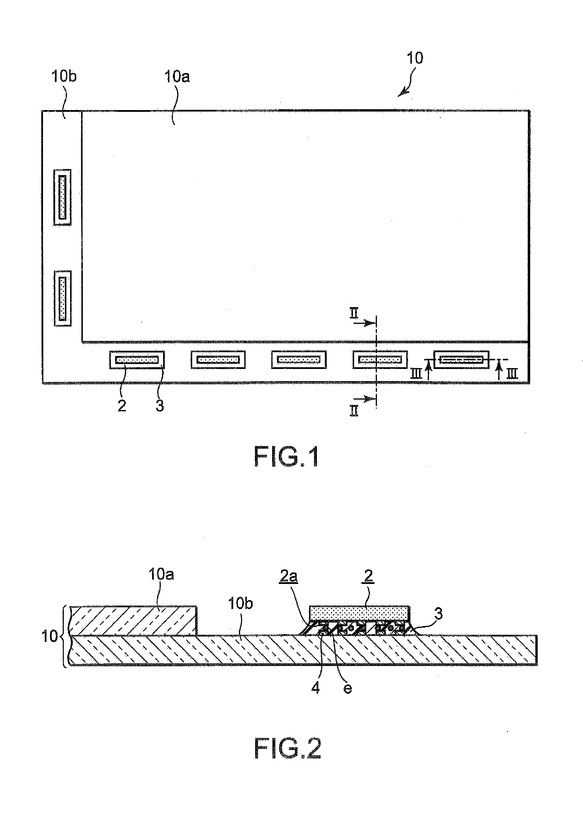
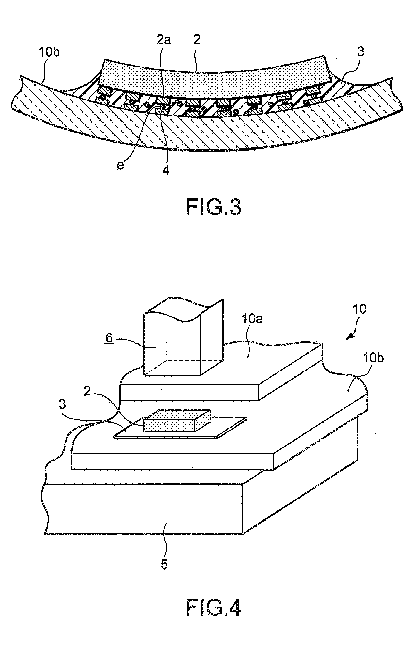
[0042]Referring to FIGS. 5 and 6, a liquid crystal display device according to the first embodiment will be described.
[0043]In the illustrated liquid crystal display device, a composite panel 1 comprises a base panel 1b made of flexible glass and having a relatively large surface area and a display panel 1a made of glass, having a relatively small surface areas and bonded to the base panel 1b with a constant gap defined therebetween. A liquid crystal layer is interposed in the gap between the base panel 1b and the display panel 1a. ICs 2 as a plurality of drive circuit components are disposed along the periphery of and spaced away from the display panel 1a, The ICs 2 are respectively fixedly bonded to the base panel 1b by an ACF 3.
[0044]Further, at predetermined portions on the base panel 1b between the display panel 1a and mounting portions of the ICs 2, quadrangular prism-shaped deformation suppression members 7a and 7b are bonded by an ordinary temperature-curable adhesive 8 alon...
second embodiment
[0061]Referring to FIG. 8, a liquid crystal display device according to the second embodiment will be described. The same portions are assigned the same reference symbols, thereby omitting explanation thereof;
[0062]The liquid crystal display device of FIG. 8 is the same in basic structure as the foregoing first embodiment. However, while use is made of the two quadrangular prism-shaped deformation suppression members 7a and 7b each being continuous and having the length approximately equal to the corresponding side of the display panel 1a in the first embodiment, quadrangular prism-shaped deformation suppression members 7c each having a length somewhat longer than that of the IC 2 in its longitudinal direction are disposed in one-to-one correspondence with the ICs 2 in the second embodiment. Thus, the number of the deformation suppression members 7c is equal to the number of the ICs 2.
[0063]According to the liquid crystal display device of the second embodiment, as compared with the...
third embodiment
[0064]Referring to FIG. 9, a liquid crystal display device according to the third embodiment will be described. The same portions are assigned the same reference symbols, thereby omitting explanation thereof.
[0065]The liquid crystal display device of FIG. 9 is the same in basic structure as the foregoing first embodiment. In the foregoing second embodiment, each of the deformation suppression members 7c provided in one-to-one correspondence with the ICs 2 surrounds the corresponding IC 2 only on the side of the display panel 1a. On the other hand, in the third embodiment, each of deformation suppression members 7d surrounds the side periphery of the corresponding a IC 2 in three directions except its outward direction such that the sectional shape of the deformation suppression member 7d in the same plane as the display surface in the height direction is a generally U-shape.
[0066]According to the liquid crystal display device of the third embodiment, since use is made of the deforma...
PUM
 Abstract
Description
Claims
Application Information