Joined body of piezoelectric single-crystal substrate and support substrate

Active Publication Date: 2021-03-04
NGK INSULATORS LTD
View PDF0 Cites 1 Cited by
  • Summary
  • Abstract
  • Description
  • Claims
  • Application Information

AI Technical Summary

Benefits of technology

[0019]When generating the amorphous layer along the bonding interface between the piezoelectric single crystal substrate and supporting substrate, the inventors then tried to change the structure of an emitting aperture of the argon atomic beam to raise the energy intensity of the argon atomic beam at the central part of the bonding interface, so that an argon concentration at the central part is made higher than a argon concentration at the peripheral part of the amorphous layer. The influences of the warping of the bonded body upon heating is then researched. As a result, it i

Problems solved by technology

Due to an increase of transmitted electric power required by recent increase of communication amount and heat generation from surrounding devices resulting from fabrication into a module, an acoustic wave filter is under the condition susceptible to high temperature.
As a result, the acoustic wave

Method used


Image

  • Joined body of piezoelectric single-crystal substrate and support substrate
  • Joined body of piezoelectric single-crystal substrate and support substrate
  • Joined body of piezoelectric single-crystal substrate and support substrate

Examples


Example

Inventive Example 1

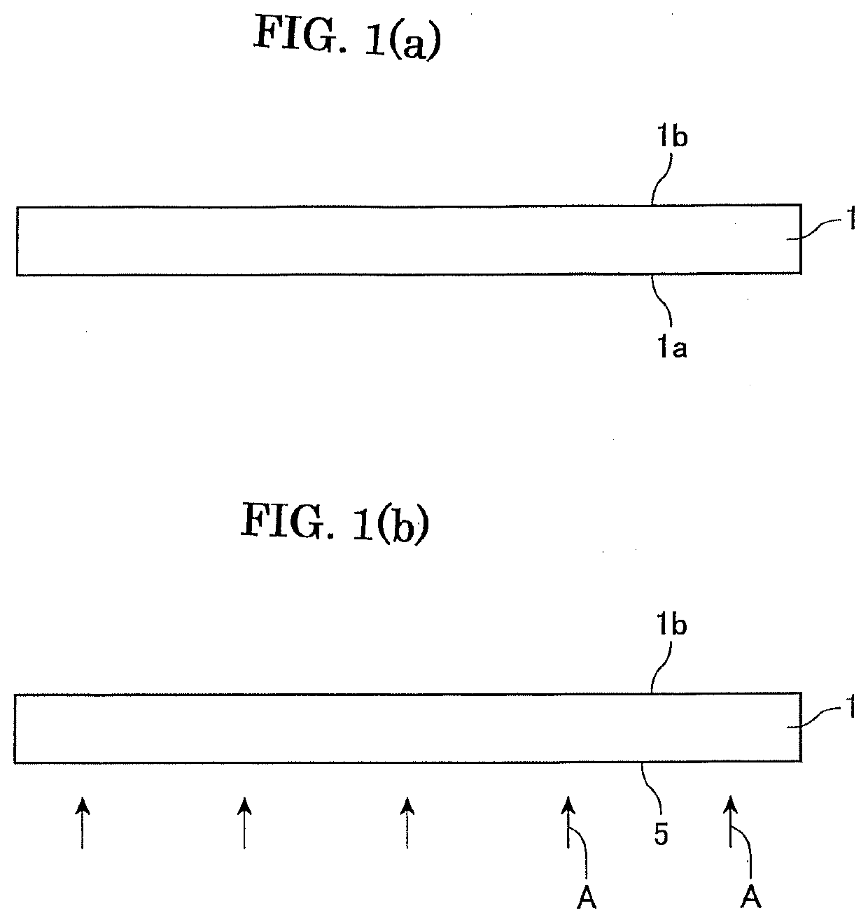
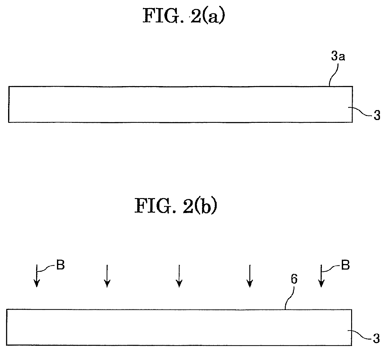
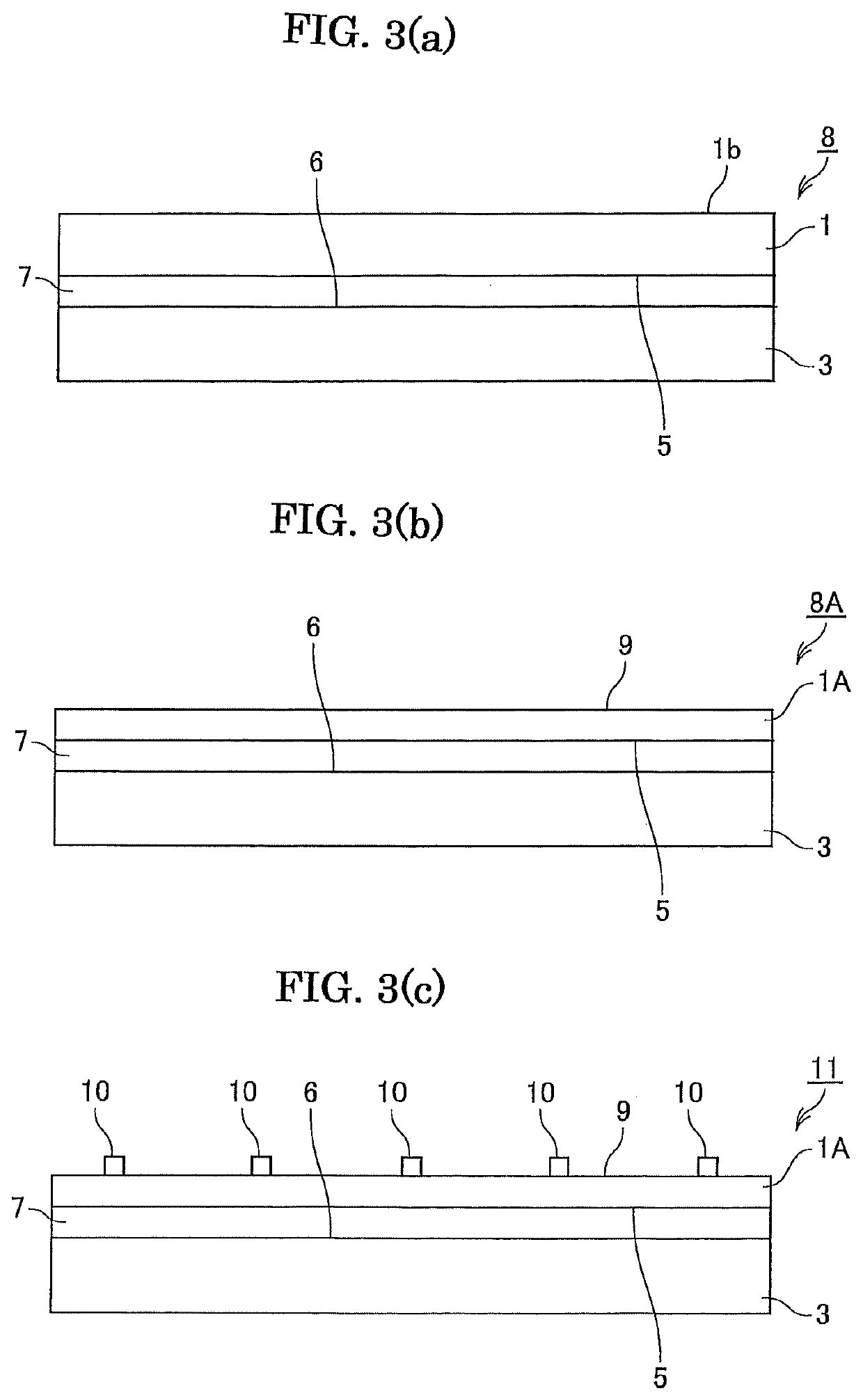
[0061]It was produced the bonded body 8A shown in FIG. 3(b), according to the method described referring to FIGS. 1 to 3.

[0062]Specifically, it was prepared a black LiTaO3 (LT) substrate (piezoelectric single crystal substrate) 1 having a thickness of 0.25 mm and of 42Y cut whose both surfaces are polished into mirror surfaces, and an Si substrate (supporting substrate) 3 having a thickness of 0.23 mm and a high resistance (≥2kΩ·cm). The sizes of the substrates were 100 mm, respectively. The surface 1a of the piezoelectric single crystal substrate 1 and surface 3a of the supporting substrate 3 were then cleaned, respectively, to remove particles from the surfaces.

[0063]The surface 1a of the piezoelectric single crystal substrate 1 and surface 3a of the supporting substrate 3 were then subjected to surface activation. Specifically, both substrates were introduced into a super-high vacuum chamber and the respective surfaces were subjected to surface activation by ar...

Example

Inventive Example 2

[0068]The bonded body 8A was produced and evaluated according to the same procedure as that of the inventive example 1. However, according to the present example, the materials of the piezoelectric single crystal substrates 1 and 1A were made lithium niobate (LN) single crystal. The results were shown in table 1 and below.

Niobium: 45.7 atom % (Central part), 41.8 atom %

(Peripheral part)

Silicon: 33.0 atom % (Central part), 38.1 atom %

(Peripheral part)

Oxygen: 17.1 atom % (Central part), 17.4 atom %

(Peripheral part)

Argon: 4.2 atom % (Central part), 2.7 atom % (Peripheral part)

Example

Comparative Example 1

[0069]The bonded body 8A was produced and evaluated according to the same procedure as that of the inventive example 1. However, according to the present example, the sizes of the grid holes at emitting aperture of the argon atomic beam were made equal in the central and peripheral parts, so that the argon atomic beam was irradiated onto the whole of the bonding surface 8A substantially uniformly. The results were shown in table 1 and below.

Tantalum: 41.5 atom % (Central part), 42.2 atom %

(Peripheral part)

Silicon: 38.4 atom % (Peripheral part), 37.6 atom %

(Peripheral part)

Oxygen: 17.7 atom % (Central part), 17.6 atom %

(Peripheral part)

Argon: 2.4 atom % (Central part), 2.6 atom % (Peripheral part)


PUM


Abstract

A bonded body includes a supporting substrate; a piezoelectric single crystal substrate composed of a material selected from the group consisting of lithium niobate, lithium tantalate and lithium niobate-lithium tantalate; and an amorphous layer present between the supporting substrate and piezoelectric material substrate, and the amorphous layer contains one or more metal atom selected from the group consisting of niobium and tantalum, an atom constituting the supporting substrate and argon atom. A concentration of the argon atom in a central part of the amorphous layer is higher than a concentration of the argon atom in a peripheral part of the amorphous layer.

Description

CROSS-REFERENCE TO RELATED APPLICATIONS[0001]This is a continuation of PCT / JP2019 / 004999, filed Feb. 13, 2019, which claims priority to Japanese Application No. JP2018-095260, filed May 17, 2018, the entire contents of which are hereby incorporated by reference.TECHNICAL FIELD[0002]The present invention relates to a bonded body of a piezoelectric single crystal substrate and supporting substrate.BACKGROUND ARTS[0003]It has been widely used an SOI substrate composed of a high resistance Si / SiO2 thin film / Si thin film, for realizing a high-performance semiconductor device. Plasma activation is used for realizing the SOI substrate. This is because the bonding can be realized at a relatively low temperature (400° C.). It is proposed a composite substrate composed of similar Si / SiO2 thin film / piezoelectric thin film for improving the performance of a piezoelectric device (patent document 1). According to patent document 1, the piezoelectric single crystal substrate composed of lithium ni...

Claims


Application Information

Patent Timeline
IPC IPC(8): H01L41/312H01L41/187H01L41/08
CPCH01L41/312H01L41/081H01L41/1873H03H9/02574H10N30/8542H10N30/072C30B29/30H03H9/25H10N30/853H10N30/086H10N30/10513
Inventor TAI, TOMOYOSHIHATTORI, RYOSUKE
Owner NGK INSULATORS LTD
Why Eureka
Try Eureka