Method of preparing high electron mobility transistor (HEMT) on large-sized Si substrate

A high electron mobility, field effect transistor technology, applied in crystal growth, chemical instruments and methods, from chemically reactive gases, etc., can solve problems such as high defect density, poor mobility of Al atoms, warping, etc. Thermal conductivity, stress and defect resolution, warpage mitigation effect

Active Publication Date: 2016-03-02
SINO NITRIDE SEMICON +1
View PDF4 Cites 8 Cited by
  • Summary
  • Abstract
  • Description
  • Claims
  • Application Information

AI Technical Summary

Problems solved by technology

[0008] However, the current mainstream insertion layer method cannot completely eliminate stress, and there are problems such as high defect density and warpage.
Moreover, the conventional ELOG (epitaxial lateral overgrowth, ELOG) technology, which is effective in reducing GaN dislocation density, is difficult to apply to AlGaN, because Al atoms have poor migration ability on the growth surface, and AlGaN will be deposited on the mask.

Method used


Image

  • Method of preparing high electron mobility transistor (HEMT) on large-sized Si substrate
  • Method of preparing high electron mobility transistor (HEMT) on large-sized Si substrate
  • Method of preparing high electron mobility transistor (HEMT) on large-sized Si substrate

Examples


Embodiment 1

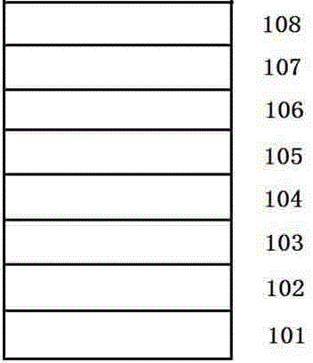
[0026] Use Aixtron company, tightly coupled vertical reaction chamber MOCVD growth system. During the growth process, trimethylgallium (TMGa) and trimethylaluminum (TMAl) were used as group III sources, ammonia (NH 3 ) as a Group V source, silane (SiH 4 ) as an n-type dopant source, dimagnesocene (Cp 2 Mg) as a p-type dopant source, the Si substrate 101 was first heated to 1080° C. in the MOCVD reaction chamber, and the 2 Under the atmosphere, use TMGa, TMAl as group III source, NH 3 As a V source, a 0.1 μm thick AlN nucleation layer was grown; then, at 1080 °C, H 2 Under the atmosphere, feed TMAl and TMGa as Group III sources, NH 3 As a group V source, a 0.5 micron thick AlGaN seed layer 102 was grown. Aligned multilayer carbon nanotubes were grown by low-pressure chemical vapor deposition (LPCVD). During the growth process, acetylene was used as the carrier gas, and 5nm Fe was used as the catalyst. The diameter of the grown carbon nanotubes is 15 nm. Through growth a...

Embodiment 2

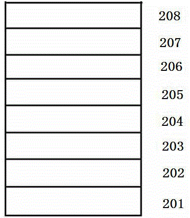
[0028] Use Aixtron company, tightly coupled vertical reaction chamber MOCVD growth system. During the growth process, trimethylgallium (TMGa) and trimethylaluminum (TMAl) were used as group III sources, ammonia (NH 3 ) as a Group V source, silane (SiH 4 ) as an n-type dopant source, dimagnesocene (Cp 2 Mg) as a p-type dopant source, the Si substrate 201 was first heated to 1080° C. in an MOCVD reaction chamber, and 2 Under the atmosphere, use TMGa, TMAl as group III source, NH 3 As a V source, a 0.1 μm thick AlN nucleation layer was grown; then, at 1080 °C, H 2 Under the atmosphere, feed TMAl and TMGa as Group III sources, NH 3 As a group V source, a 0.5 micron thick AlGaN seed layer 202 was grown. Aligned multilayer carbon nanotubes were grown by low-pressure chemical vapor deposition (LPCVD). During the growth process, acetylene was used as the carrier gas, and 5nm Fe was used as the catalyst. The diameter of the grown carbon nanotubes is 15 nm. Through growth and we...


PUM

PropertyMeasurementUnit
thicknessaaaaaaaaaa

Abstract

The invention provides a method of preparing a high electron mobility transistor (HEMT) on a large-sized Si substrate, and particularly relates to a method of preparing a crack-free and high-crystal quality AlGaN/GaN HEMT device by adopting a selective area growth (SAG) method and by adopting carbon nanotubes as a periodic dielectric mask. On the Si substrate, a metal organic chemical vapor phase epitaxy technology is adopted to grow an AlN nucleation layer and an AlGaN seed layer; then, a low pressure chemical vapor deposition (LPCVD) method is adopted to grow multiple layers of carbon nanotubes arranged neatly, and through growth and weaving, a continuous carbon nanotube film is formed finally; on the basis, the SAG method is adopted, growth selectivity of GaN on the dielectric mask and the substrate is used, a GaN epitaxial layer is limited to grow in a region without a concealed film, a discrete window is formed, and tensile stress in the overall epitaxial layer is released; and multi-cycle Al component-gradient Aly1Ga1-y1N/GaN superlattices or AlN/Aly1Ga1-y1N/GaN superlattices are adopted as a stress control layer, and the crack-free and high-crystal quality GaN epitaxial layer is acquired. On the basis, the AlGaN/GaN HEMT device is prepared.

Description

technical field [0001] The invention relates to a method for preparing a high electron mobility [field effect] transistor (HEMT, highelectronmobilitytransistor) on a large-size Si substrate. In particular, it relates to a method for preparing AlGaN / GaN HEMT devices with no cracks and high crystal quality by using carbon nanotubes as a periodic dielectric mask and using a selective area growth (SAG) method, which belongs to the field of semiconductor optoelectronic technology. Background technique [0002] High electron mobility field effect transistor (HEMT), also known as modulation-doped field effect transistor (MODFET, modulation-doped field effect transistor), is a two-dimensional electron gas with a heterogeneous interface formed by a substrate material and another broadband material. Conductive Field Effect Transistor (FET). Because there are no impurities in the channel, there is basically no impact of ionized impurity scattering on electron movement, so the electron...

Claims


Application Information

Patent Timeline
Patent Type & Authority Applications(China)
IPC IPC(8): H01L21/335H01L21/205C23C16/26C30B25/04
Inventor 张国义贾传宇
Owner SINO NITRIDE SEMICON
Why Eureka
Try Eureka