Semiconductor assembly, seal ring structure and forming method thereof

A technology of guide holes and metal wires, which is applied in the field of semiconductor integrated circuits, can solve problems such as short circuits and loss of function of aluminum pads 140, and achieve the effects of avoiding stress damage and improving the pass rate

Active Publication Date: 2007-07-18
TAIWAN SEMICON MFG CO LTD
View PDF0 Cites 11 Cited by
  • Summary
  • Abstract
  • Description
  • Claims
  • Application Information

AI Technical Summary

Problems solved by technology

In addition, the process of forming bumps or other IC patterns before dicing the wafer, such as chemical etching, will make the residual aluminum pad 140 useless.
The remaining aluminum pads cause serious negative effects such as short circuit and parasitic capacitance in the fabricated components, or become conductive channels between IC patterns (such as bumps) to short circuit

Method used


Image

  • Semiconductor assembly, seal ring structure and forming method thereof
  • Semiconductor assembly, seal ring structure and forming method thereof
  • Semiconductor assembly, seal ring structure and forming method thereof

Examples


Embodiment Construction

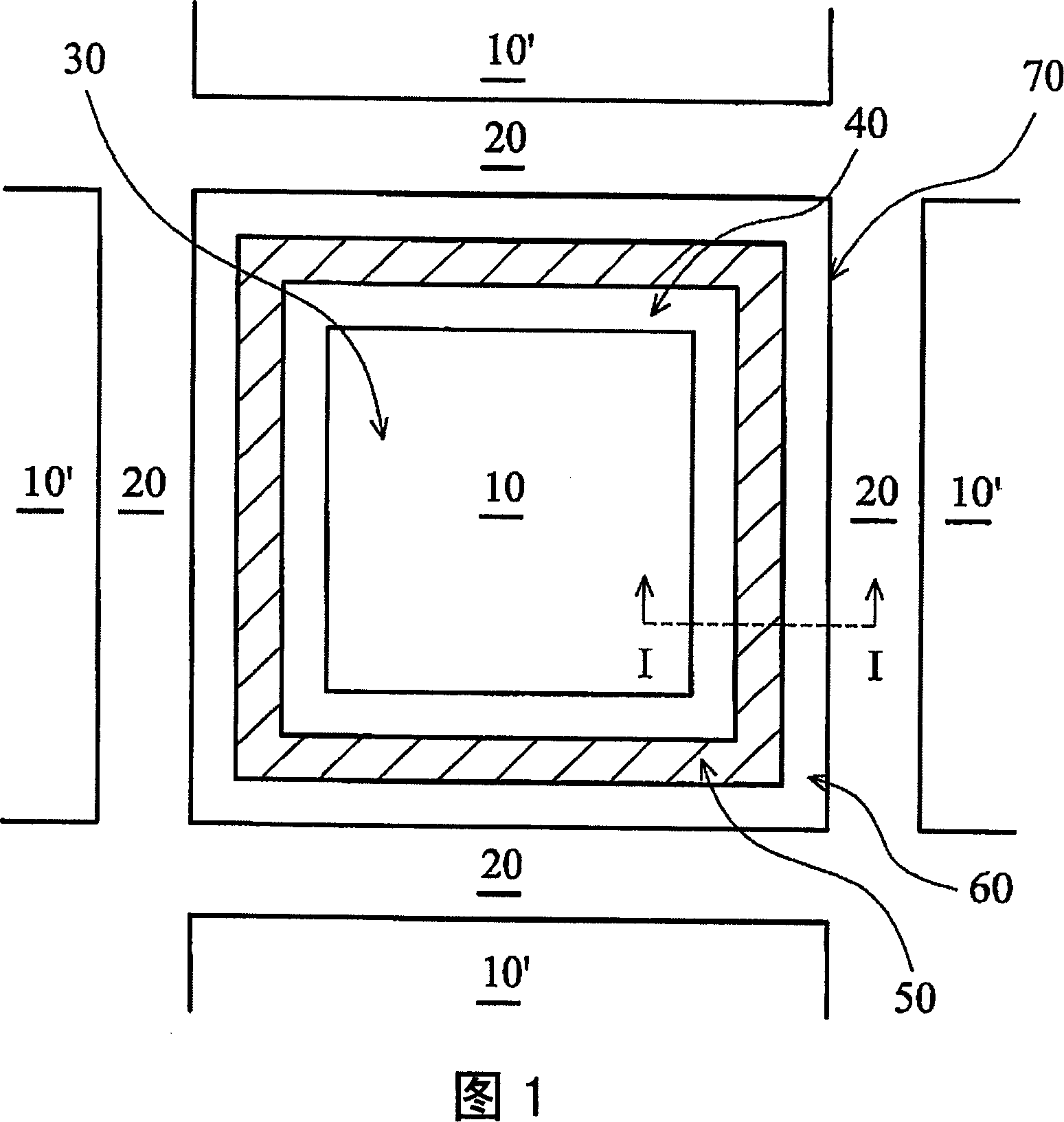
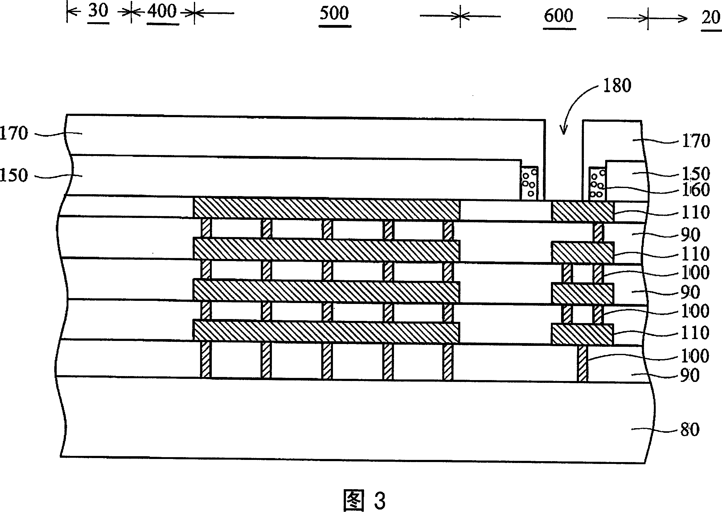
[0033] As shown in FIG. 3 , it is a cross-sectional view of the sealing ring structure of the embodiment of the present invention. As shown, the integrated circuit 30 is formed on a silicon substrate 80 . The silicon substrate 80 may have components, junctions, or other components (not shown). For example, a field oxide layer (as shown) can be formed between the sealing ring structure (the first sealing ring 600 , the second sealing ring 500 , and the isolation region 400 ) and the integrated circuit 30 . The second sealing ring 500 has metal layers 110 and dielectric layers 90 stacked alternately, and the two are electrically connected by via plugs 100 . A preferred dielectric layer can be a material with a low dielectric constant (dielectric constant less than 3.9), and the formation method can be a known deposition process such as chemical vapor deposition (hereinafter referred to as CVD). In the present invention, the function of the guide hole plug is to reduce the stre...


PUM


Abstract

A seal ring structure between an integrated circuit region and a scribe line is provided. In one embodiment, the seal ring structure comprises a substrate; a plurality of layers of metal lines formed overlying the substrate; a plurality of via plugs through intermetal dielectric layers between the layers of metal lines and wherein the via plugs interconnect the metal lines; a first passivation layer formed over the plurality of layers of metal lines, the first passivation layer having an opening therein exposing a portion of a top metal line; residual metal pad layers formed proximal the opening of the first passivation layer; and a second passivation layer formed over the first passivation layer, the second passivation layer enveloping the exposed residual metal pad or metal redistribution layers and further having a trench above the top metal line.

Description

technical field [0001] The present invention relates to a semiconductor integrated circuit, more particularly to a sealing ring structure, which is used to reduce the stress generated when cutting chips. Background technique [0002] In semiconductor manufacturing methods, areas on a wafer are divided into chips with integrated circuits, and dicing streets that separate the chips. Cutting along the dicing lines separates the entire wafer into dies. [0003] However, the lateral stress generated during the cutting process will affect the structure of the integrated circuit, and the generated microcracks will eventually reduce the process efficiency. The solution is to form a sealing ring structure between the dicing line and the periphery of the integrated circuit. The known sealing ring structure is a metal connection connected by a line-type via. FIG. 1 is a top view of a conventional sealing ring structure surrounding a certain chip before wafer dicing. The scribe line...

Claims


Application Information

Patent Timeline
Patent Type & Authority Applications(China)
IPC IPC(8): H01L27/02H01L23/00H01L21/82
CPCH01L2924/0002H01L23/3192H01L23/585H01L2924/00
Inventor 杨肇祥
Owner TAIWAN SEMICON MFG CO LTD
Why Eureka
Try Eureka