Method and circuit for electrically programming semiconductor memory cells

a technology of semiconductor memory cells and circuits, applied in the field of solid-state memories, can solve the problems of generating several reference currents/voltages, no longer verifying the programming state, and generating different reference voltages/currents within the memory devi

Active Publication Date: 2008-01-17
MICRON TECH INC
View PDF3 Cites 20 Cited by
  • Summary
  • Abstract
  • Description
  • Claims
  • Application Information

AI Technical Summary

Benefits of technology

[0023] After the reaching of a target programming state by the memory cells is assessed, at least one further electrical programming pulse is applied to the memory cell, and the reaching of a target programming state is verified at least one more time after applying the further programming pulse. In case, as a result of said further verify, the reaching of the target programming state by the memory cell is not assessed, the method provides for applying a still further programming pulse to the memory cell.
[0024] Thus, the method programs memory cells, particularly non-volatile memory cells, which, differently from the conventional programming methods, does not inhibit the execution of program verify operations on memory cells that have already been assessed to have reached the target programming state: every memory cell in a group of memory cells under programming continues to be subject to program verify operations, until all the memory cells are assessed as programmed to the respective target programming state, and the program operation is completed.

Problems solved by technology

The Applicant has observed that the way the program operation is usually conducted may cause problems.
In particular, the Applicant has observed that problems may arise from the fact that a memory cell, immediately after having been verified as correctly programmed to the target programming state, is permanently excluded from being applied further programming pulses, and its programming state is no longer verified.
This has the disadvantage that different reference voltages / currents need to be generated within the memory device for the use in a normal read operation and for the use in a program verify operation.
Having to generate several reference current / voltages is disadvantageous, because several reference circuit structures need to be integrated and trimmed, e.g., during the memory device testing.
This increases the costs.
Also, dispensing a memory cell from being subjected to further verify operations right after it has been verified as programmed to the target state is risky: due to the change in biasing conditions that inevitably takes place due to the programming of the remaining memory cells, that memory cell, initially verified as correctly programmed, might, at a later time, e.g., after completion of the programming operation on the remaining memory cells, be seen as not programmed.
If this occurs, the functioning of the memory device is impaired, because incorrect data are stored therein.

Method used


Image

  • Method and circuit for electrically programming semiconductor memory cells
  • Method and circuit for electrically programming semiconductor memory cells
  • Method and circuit for electrically programming semiconductor memory cells

Examples


Embodiment Construction

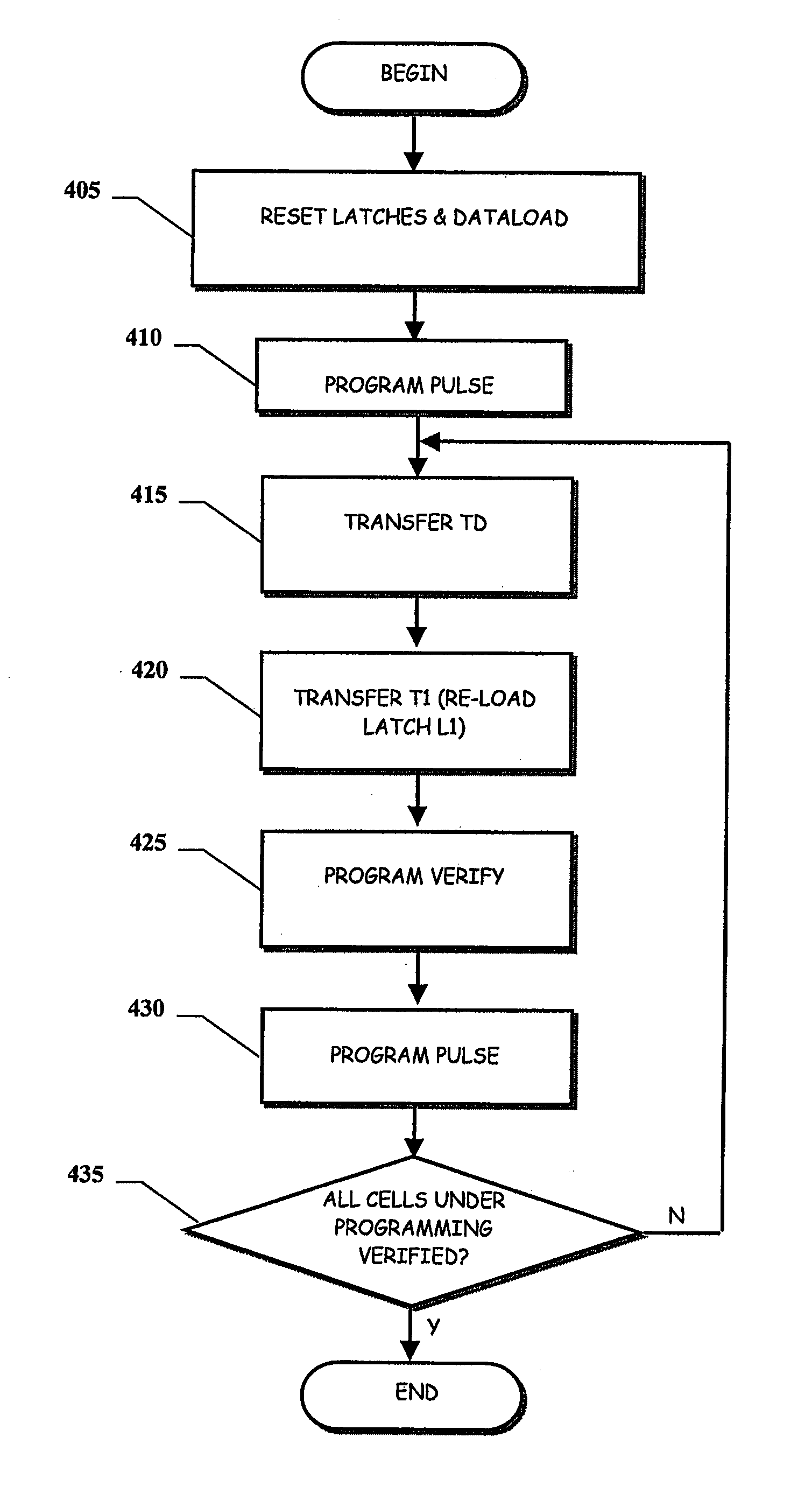
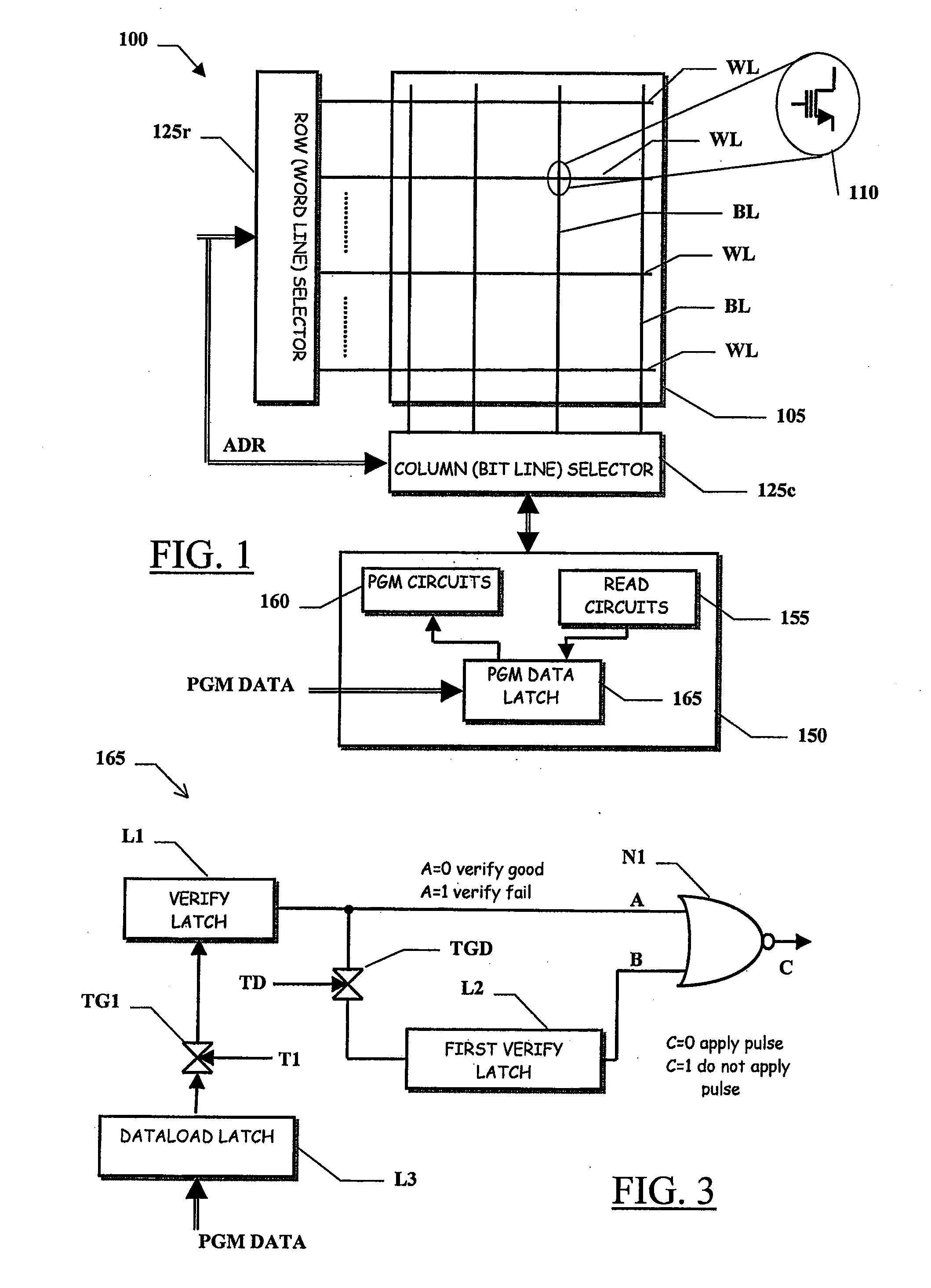
[0042] With reference to the drawings, in FIG. 1 a non-volatile semiconductor memory, globally identified as 100, is schematically illustrated in terms of the main functional blocks; in particular, the memory 100 is an electrically-programmable, non-volatile semiconductor memory, for example a flash memory.

[0043] The flash memory 100 is integrated in a chip of semiconductor material, and includes a plurality of memory cells 110 adapted to store data; the memory cells 110 are arranged in a plurality of rows and a plurality of columns, and form a two-dimensional memory matrix 105.

[0044] Typically, each memory cell 110 consists of or includes an N-channel MOS transistor having a charge-storage element, such as a conductive, electrically-insulated floating-gate electrode adapted to be charged by electrons.

[0045] The flash memory 100, and particularly the memory matrix 105 may either have a NOR architecture or a NAND architecture, the specific architecture of the flash memory 100 bein...


PUM


Abstract

A method of electrically programming a memory cell includes: applying at least one electrical programming pulse to the memory cell; verifying the reaching of a target programming state by the memory cell; and repeating the acts of applying and verifying until the reaching of a target programming state by the memory cell is assessed. After the reaching of a target programming state by the memory cells is assessed, at least one further electrical programming pulse is applied thereto, and the memory cell is verified at least one more time after applying the further programming pulse. In case, as a result of said further verifying, the reaching of the target programming state by the memory cell is not assessed, the method provides for applying a still further programming pulse to the memory cell.

Description

BACKGROUND [0001] 1. Technical Field [0002] The present invention generally relates to the field of solid-state memories, particularly to semiconductor memories and, even more particularly, to non-volatile semiconductor memories. Specifically, the invention relates to the class of non-volatile memories that are electrically programmable, i.e., the information content of which can be altered electrically. [0003] 2. Description of the Related Art [0004] Non-volatile memory devices (shortly, non-volatile memories) are commonly used in several applications, when it is needed or desired that the data stored in the memory device are preserved even in absence of power supply. [0005] Within the class of non-volatile memories, electrically alterable memories, particularly electrically programmable and erasable memories, such as Flash memories, have become very popular in those applications where the data to be stored are not immutable, being instead desirable from time to time to store new d...

Claims


Application Information

Patent Timeline
Patent Type & Authority Applications(United States)
IPC IPC(8): G11C16/10G11C7/00
CPCG11C11/5628G11C16/0483G11C2211/5621G11C16/3459G11C16/3454
Inventor CRIPPA, LUCAMICHELONI, RINO
Owner MICRON TECH INC
Why Eureka
Try Eureka