Rigid-flexible printed circuit board and method of manufacturing the same

a printed circuit board, rigid technology, applied in the direction of cross-talk/noise/interference reduction, lithographic masks, etching metal masks, etc., can solve the problems of high cost of processing, high cost of applying and removing resists, high manufacturing cost, etc., to eliminate the cost of previously processing, easy to perform

Inactive Publication Date: 2008-01-17
SAMSUNG ELECTRO MECHANICS CO LTD
View PDF7 Cites 58 Cited by
  • Summary
  • Abstract
  • Description
  • Claims
  • Application Information

AI Technical Summary

Benefits of technology

[0020]Accordingly, the present invention has been made to solve the above problems occurring in the prior art, and an object of the present invention is to provide a rigid-flexible printed circuit board and a method of manufacturing the same, in which coverlays are layered on the entire surface of a double-sided FCCL without previous processing thereof, via holes are formed in the coverlays while a drilling process is performed to form the via holes, and then copper plating is performed over the entire surface thereof, thereby eliminating the cost of previously processing the coverlays, easily performing a process of provisionally layering the coverlays on the double-sided FCCL, and decreasing the cost thereof.

Problems solved by technology

However, since, in the conventional rigid-flexible printed circuit board, the windows are formed in the coverlays through previous processing, there have been problems in that manufacturing cost is high, and the process of layering the coverlays on the double-sided FCCL in to conform to the inner circuit patterns respectively formed on the two sides of the double-sided FCCL is difficult, and thus the cost of performing the processing is high.
Further, there have been problems in that the cost of applying and removing the resists is high, and defects may occur because residual resist is present on the circuit pattern after removal of the resists.

Method used


Image

  • Rigid-flexible printed circuit board and method of manufacturing the same
  • Rigid-flexible printed circuit board and method of manufacturing the same
  • Rigid-flexible printed circuit board and method of manufacturing the same

Examples


first embodiment

[0052]FIG. 3 is a flow chart schematically showing a method of manufacturing a rigid-flexible printed circuit board according to the present invention.

[0053]The method of manufacturing a rigid-flexible printed circuit board according to the first embodiment of the present invention is performed through the following steps.

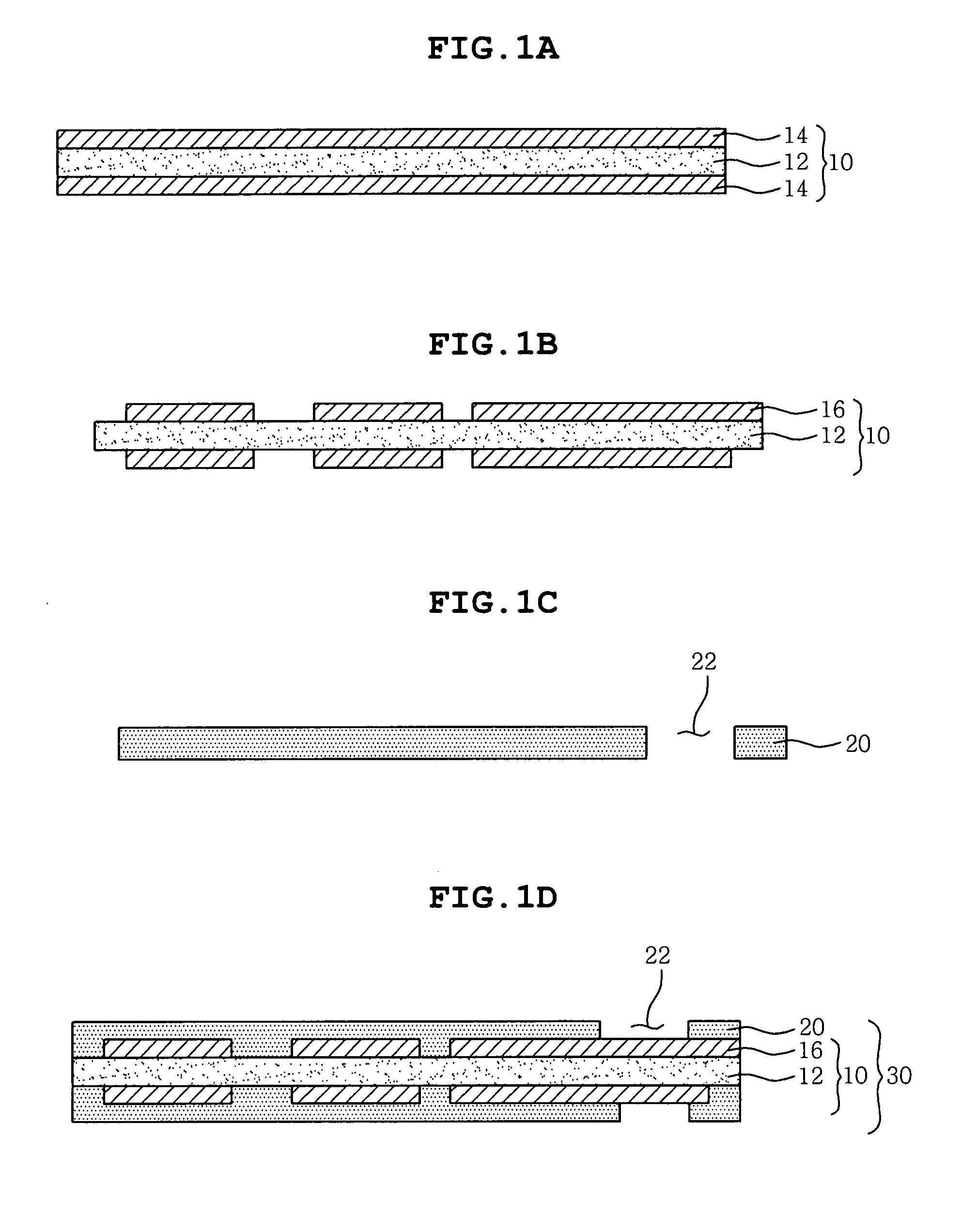
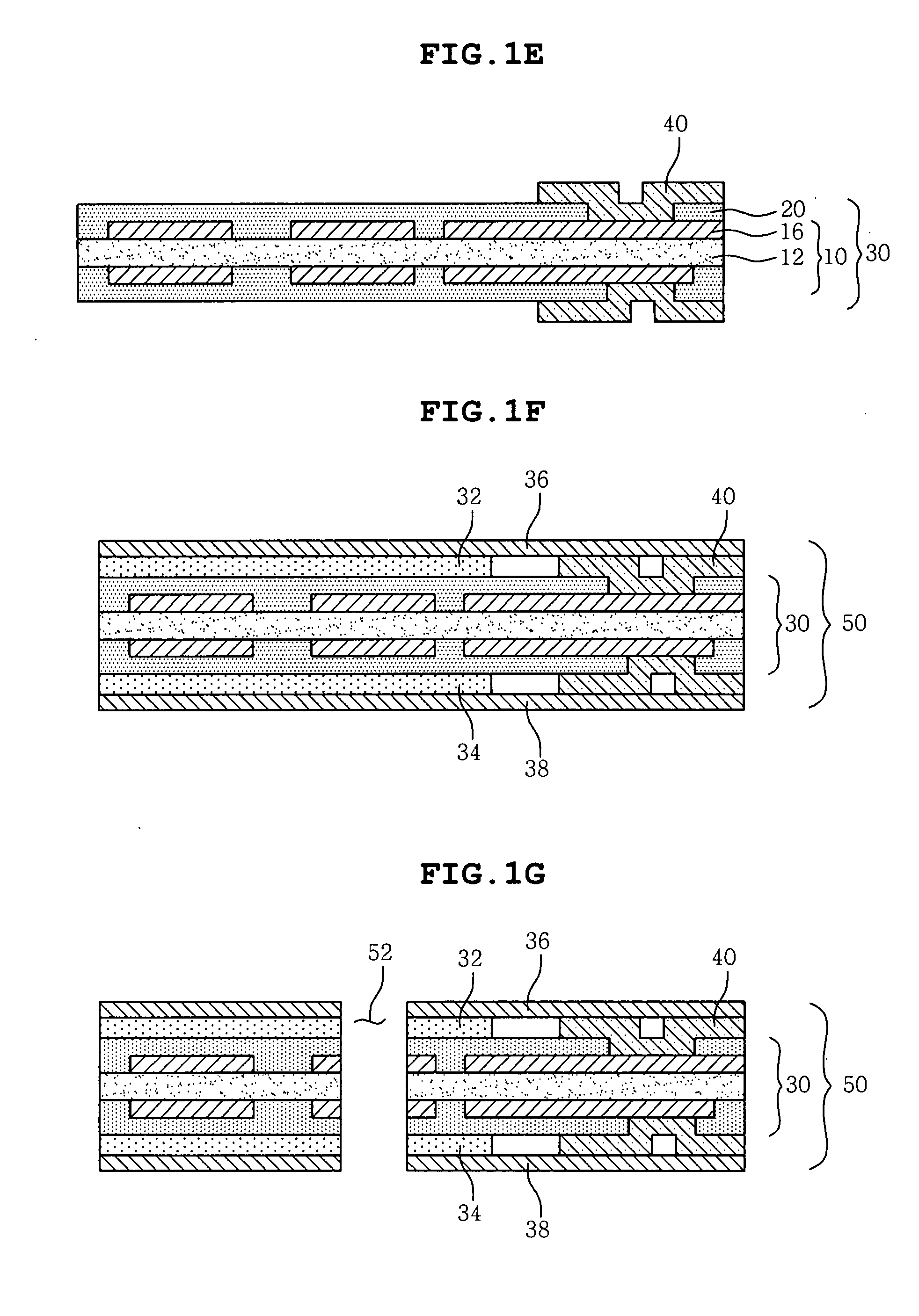
[0054]First, a base substrate, in which coverlays are formed over two sides of a double-sided FCCL on both sides of which inner circuit patterns are formed, is provided (S110). Insulation layers and copper foil layers are layered on the portions of coverlays which are to be a rigid region of the double-sided FCCL (S120). A via hole is formed in the rigid region using a CO2 laser, and simultaneously first windows are formed in the coverlays of the flexible region (S130).

[0055]An entire plating layer is formed over the entire area, and outer circuit patterns including a region around the first window are formed from the plating layer (S140). Then, solder resists are ...

second embodiment

[0071]FIG. 5 is a flow chart schematically showing a method of manufacturing a rigid-flexible printed circuit board according to the present invention.

[0072]The method of manufacturing a rigid-flexible printed circuit board according to the second embodiment of the present invention is performed through the following steps.

[0073]First, a base substrate, in which coverlays are respectively formed on two sides of a double-sided FCCL on both sides of which inner circuit patterns and first windows are respectively formed, is provided (S210). Insulation layers and copper foil layers are layered on the portions of coverlays which are to be the rigid region of the double-sided FCCL (S220). A via hole is formed in the rigid region using a CO2 laser and, simultaneously, another via hole is formed to correspond to the first window in the flexible region (S230).

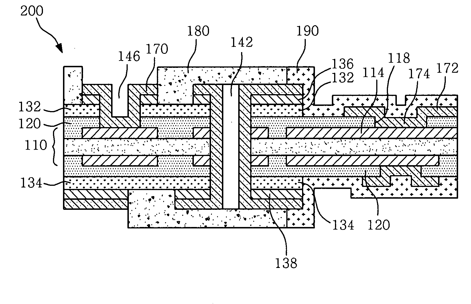
[0074]An entire plating layer is formed over the entire area, and outer circuit patterns including a region around the first window ar...

third embodiment

[0094]FIG. 7 is a flow chart schematically showing a method of manufacturing a rigid-flexible printed circuit board according to the present invention.

[0095]The method of manufacturing a rigid-flexible printed circuit board according to the third embodiment of the present invention is performed through the following steps.

[0096]First, a base substrate, in which coverlays are respectively formed on two sides of a double sided FCCL, on both sides of which inner circuit patterns and first window are formed, is provided (S310). Insulation layers and copper foil layers are respectively layered on the portions of coverlays which are to be a rigid region of the base substrate (S320). A via hole is formed in the rigid region using an ultraviolet laser, and simultaneously another via hole is formed in the flexible region (S330).

[0097]An entire plating layer is formed over the entire area, and outer circuit patterns including a region around the via holes are formed from the plating layer (S3...


PUM

PropertyMeasurementUnit
flexibleaaaaaaaaaa
diametersaaaaaaaaaa
diameteraaaaaaaaaa

Abstract

The present invention relates to a rigid-flexible printed circuit board and, more particularly, to a rigid-flexible printed circuit board including CL via holes which can facilitate electrical connection to an inner circuit pattern in a flexible region. Since the coverlays are layered on the entire surface of the double-sided FCCL without previous processing thereof, the via holes are formed in the coverlays while a drilling process is performed to form the via holes, and then the copper plating is performed over the entire surface thereof, it is possible to eliminate the cost of previously processing the coverlays, easily perform a process of provisionally layering the coverlays on the double-sided FCCL, and decrease the cost therefor.

Description

CROSS REFERENCE TO RELATED APPLICATION[0001]This application claims the benefit of Korean Patent Application No. 10-2006-0065847, filed Jul. 13, 2006, entitled “Rigid-flexible printed circuit board and manufacturing method therefor”, which is hereby incorporated by reference in its entirety into this application.BACKGROUND OF THE INVENTION[0002]1. Field of the Invention[0003]The present invention relates to a rigid-flexible printed circuit board and, more particularly, to a rigid-flexible printed circuit board including CL via holes which can facilitate electrical connection to an inner circuit pattern in a flexible region.[0004]2. Description of the Related Art[0005]Generally, a rigid-flexible printed circuit board is formed by structurally combining a rigid substrate, which is made of a rigid material, with a film type flexible substrate, which can be easily bent. In the rigid-flexible printed circuit board, the rigid substrate is connected with the flexible substrate without an a...

Claims


Application Information

Patent Timeline
Patent Type & Authority Applications(United States)
IPC IPC(8): H05K1/00H05K3/00
CPCH05K1/0218Y10T29/49124H05K3/281H05K3/429H05K3/4644H05K3/4652H05K3/4664H05K3/4691H05K2201/0195H05K2201/0715H05K2201/09509H05K2203/054H05K2203/0554Y10T29/49165Y10T29/49126Y10T29/49158Y10T29/49169Y10T29/49128Y10T29/49171Y10T29/49155H05K3/0035H05K1/02
Inventor LEE, YANG JESHIN, IL WOONKIM, GOING SIKHONG, DOO PYOKIM, HA ILAN, DONG GI
Owner SAMSUNG ELECTRO MECHANICS CO LTD
Why Eureka
Try Eureka