Method of deep etching

a deep etching and etching technology, applied in the field of deep etching, can solve the problems of critical dimension bias and less precision, unstable etching conditions, disorganized etching parameters, etc., and achieve the effect of less critical dimension bias and flexibility, good anisotropic features, and forming delicate mems devices

Inactive Publication Date: 2008-01-31
TOUCH MICRO SYST TECH
View PDF8 Cites 19 Cited by
  • Summary
  • Abstract
  • Description
  • Claims
  • Application Information

AI Technical Summary

Benefits of technology

[0008]The method of the present invention has advantages of good-anisotropic features, less critical dimension bias and flexibility, and is able to form delicate MEMS devices.

Problems solved by technology

The conventional DRIE process encounters problems of disarranged etching parameters, unstable etching conditions, or undesirable effects resulting from the lattice structure of the silicon wafer 10.
The structural flaw will result in problems of critical dimension (CD) bias and less precision.

Method used


Image

  • Method of deep etching
  • Method of deep etching
  • Method of deep etching

Examples


Embodiment Construction

[0013]In the following detailed description, reference is made to the accompanying drawings, which form a part of this application. The drawings show, by way of illustration, specific embodiments in which the invention may be practiced. It is to be understood that other embodiments may be utilized and structural changes may be made without departing from the scope of the present invention.

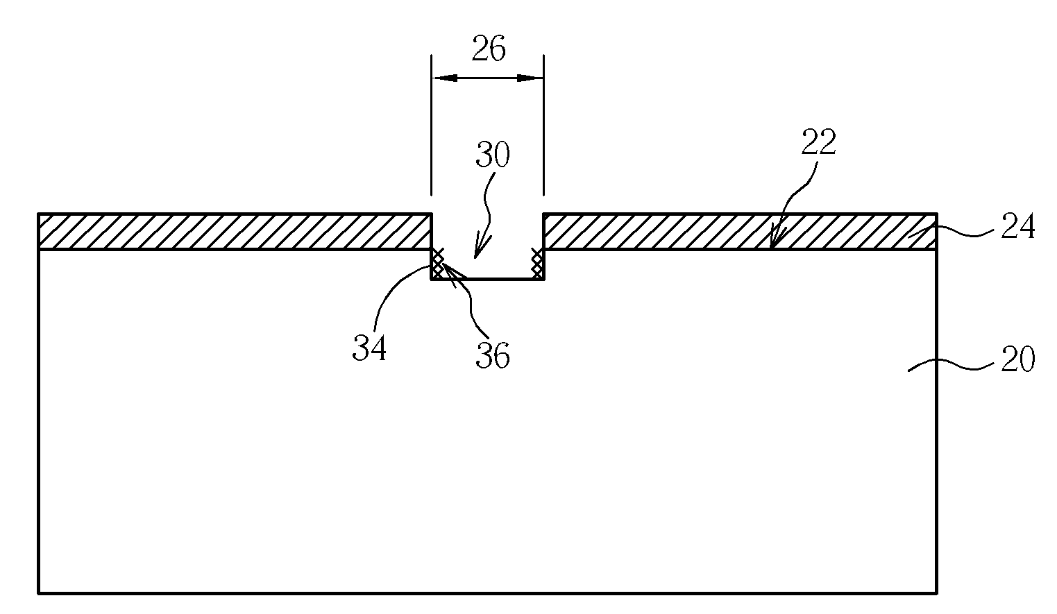
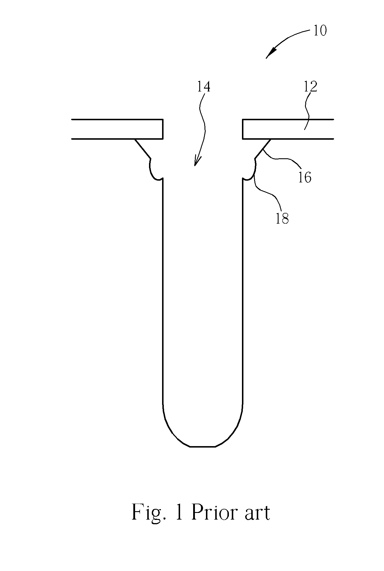
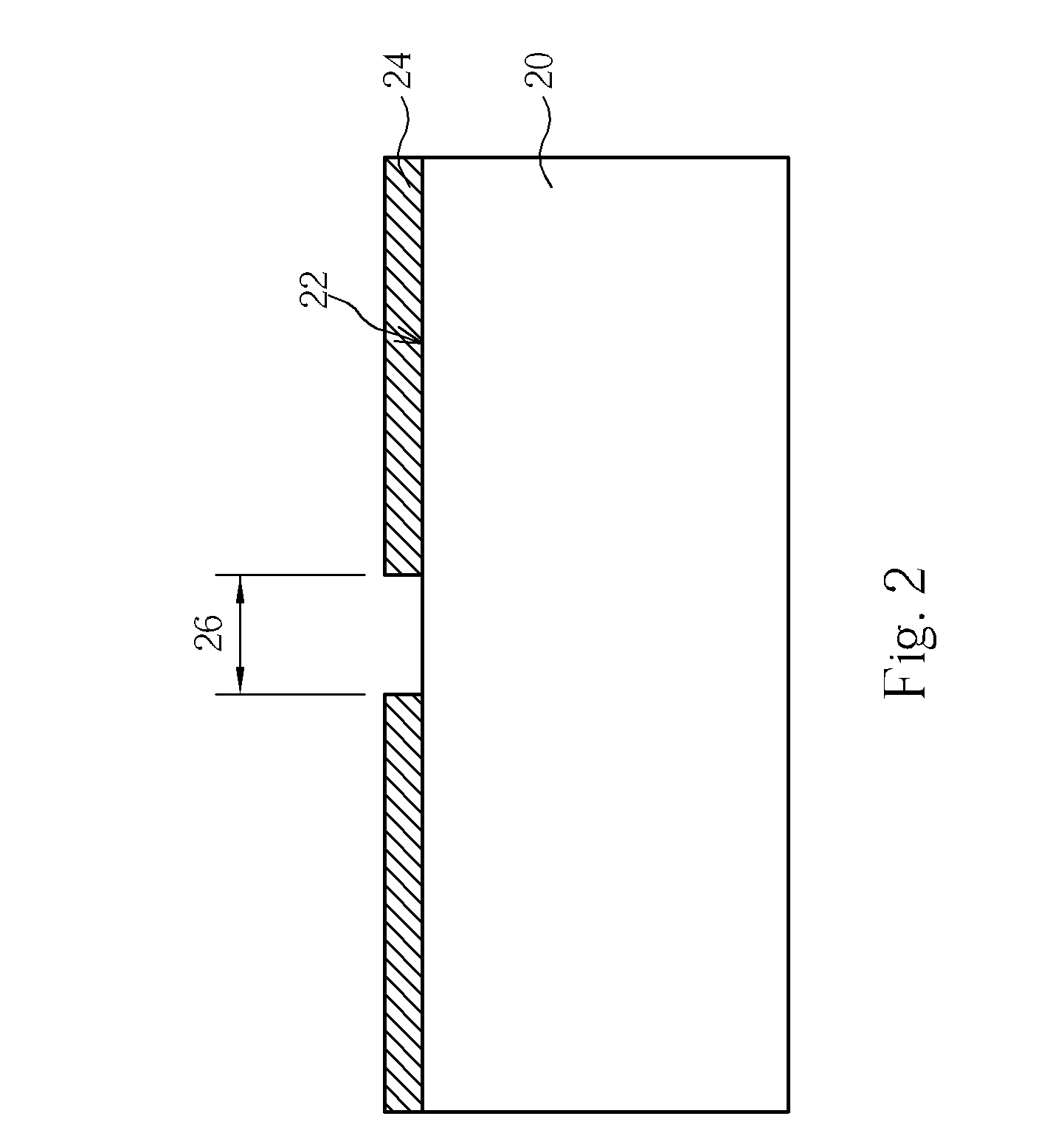
[0014]FIGS. 2 to 5 are schematic diagrams illustrating a method of deep etching according to a preferred embodiment of the present invention. As shown in FIG. 2, a wafer 20 is provided. A patterned mask 22 having at least an opening 26 is formed on a surface 22 of the wafer 20. The opening 26 exposes the surface 22 of the wafer and defines the position of a deep opening formed in the following processes. The wafer 22 is a silicon wafer and other kinds of wafers can also be used, for instance, a single crystalline silicon wafer, an amorphous crystalline silicon wafer, or a poly crystalline silicon w...


PUM

PropertyMeasurementUnit
RF poweraaaaaaaaaa
RF poweraaaaaaaaaa
aspect ratioaaaaaaaaaa

Abstract

A method of deep etching is disclosed. Initially, a wafer is provided, and a patterned mask having at least an opening to expose a surface of the wafer is formed on the surface of the wafer. A deposition process is performed to form a polymer layer on the patterned mask and a part of the surface through the opening. And accordingly, a plasma etching process is performed to remove the polymer layer and to etch the surface through the opening to form a deep opening. An oxide layer is formed on a sidewall of the deep opening to protect the sidewall during the plasma etching process. The deposition process and the plasma etching process are repeated alternatively until the deep opening has a predetermined aspect ratio. The method of the invention etches the wafer anisotropically and forms a deep opening having a hydrophilic surface of the sidewall.

Description

BACKGROUND OF THE INVENTION [0001]1. Field of the Invention[0002]The present invention is related to a method of deep etching, and particularly to a method of deep etching in which a deposition process and a plasma etching process are repeated alternatively.[0003]2. Description of the Prior Art[0004]Micro-electromechanical system (MEMS) devices are tiny 3D-structures, such as circuits, sensors, and actuators, formed on wafers by microminiaturization technology, and are able to make difficult actions. MEMS technology is a multi-disciplinary integrated technology based on integrated circuits and other techniques including electronics, mechanics, optics, and material science etc. The structure of MEMS device includes immobile structures, such as probes, openings or holes; or mobile structures, such as springs, shafts, or gear wheels. The above-mentioned MEMS structures may be formed by wafer-bonding and bulk micromachining to form micro-fluid structures. At present, the MEMS technology...

Claims


Application Information

Patent Timeline
Patent Type & Authority Applications(United States)
IPC IPC(8): C03C25/68C23F1/00
CPCB81C1/00571H01L21/30655B81C2201/0132
Inventor TSAI, TE-KENG
Owner TOUCH MICRO SYST TECH
Why Eureka
Try Eureka