Storage nodes, phase change memories including a doped phase change layer, and methods of operating and fabricating the same

Inactive Publication Date: 2008-01-31
SAMSUNG ELECTRONICS CO LTD
View PDF2 Cites 8 Cited by
  • Summary
  • Abstract
  • Description
  • Claims
  • Application Information

AI Technical Summary

Benefits of technology

[0014] Example embodiments may provide a phase change memory having a doped phase change layer that may have a lowered reset current, a lowered melting point, and / or an increased resistance.

Problems solved by technology

Because the drive current of a transistor may be determined by its size, it may be difficult to reduce the size of the transistor without reducing the reset current.
Increase in PRAM integration may be difficult without reducing the reset current.

Method used


Image

  • Storage nodes, phase change memories including a doped phase change layer, and methods of operating and fabricating the same
  • Storage nodes, phase change memories including a doped phase change layer, and methods of operating and fabricating the same
  • Storage nodes, phase change memories including a doped phase change layer, and methods of operating and fabricating the same

Examples


example embodiment

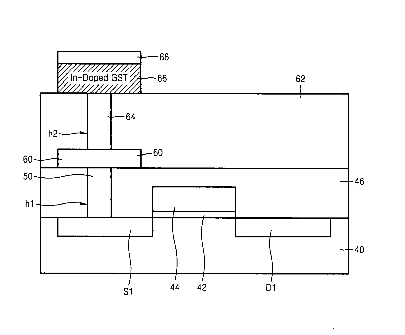
[0040] Example embodiment phase change memories may write and / or read data if a reset current smaller than about 1 mA is applied to the phase change layer 66 of the phase change memory.

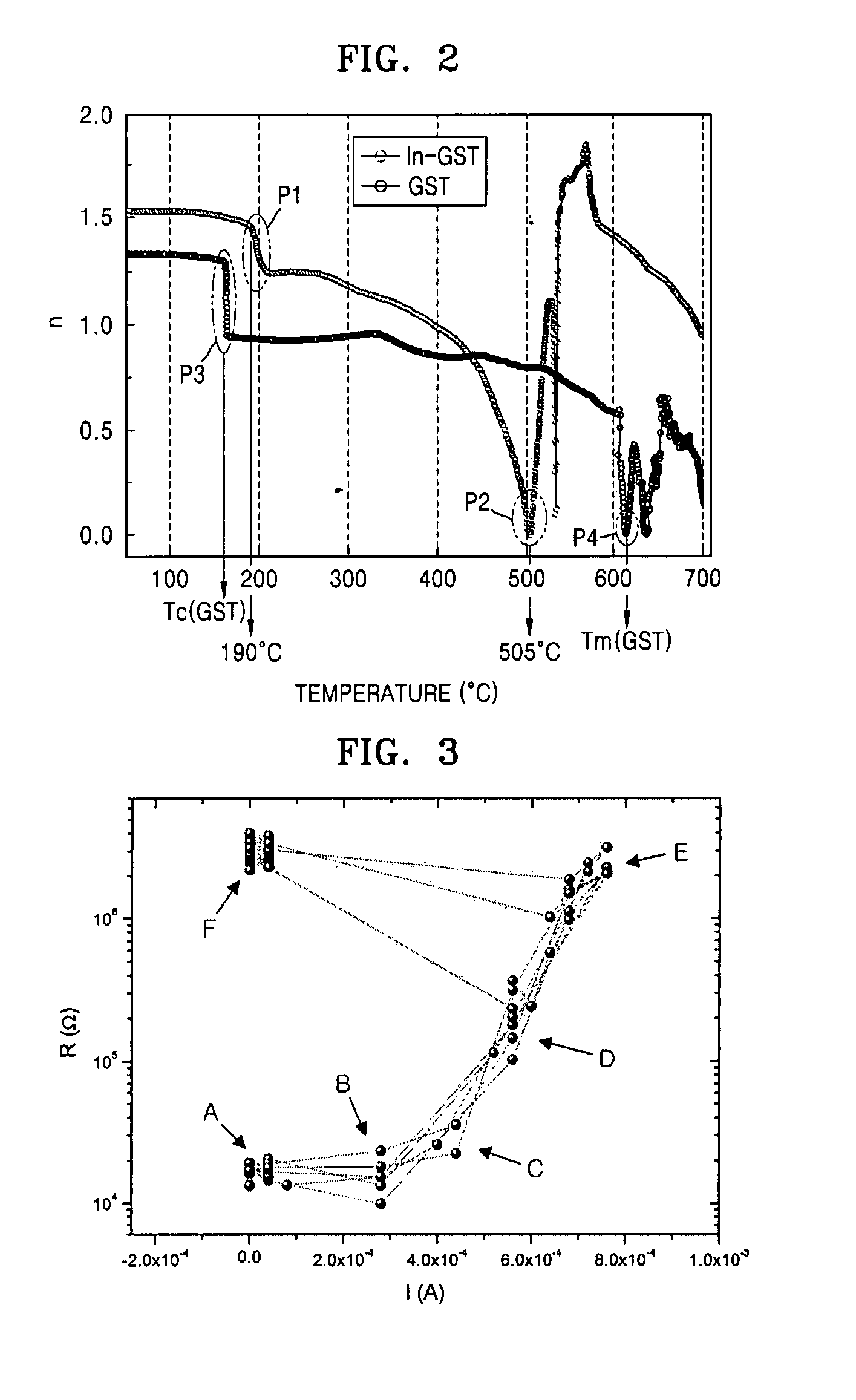
[0041]FIG. 2 is graph illustrating characteristic refractive index versus temperature of the phase change layer 66. A first graph G1 shows the refractive index versus temperature of a phase change layer 66 used in an example embodiment phase change memory, and a second graph G2 shows the refractive index versus temperature of a GST layer used in a related art phase change memory.

[0042] As shown in the first graph G1, the refractive index may be drop at a first point P1 and continue to drop to a second point P2. However, the refractive index may increase at the second point P2. The first point P1 may appear due to a transformation of the phase change layer 66 from an amorphous state into a crystalline state. The second point P2 may appear due to a transformation of a portion of the phase change layer ...


PUM


Abstract

Example embodiments may provide a doped phase change layer and a method of operating and fabricating a phase change memory with the example embodiment doped phase change layer. The phase change memory may include a storage node having a phase change layer and a switching device, wherein the phase change layer includes indium with a concentration ranging from about 5 at % to about 15 at %. The phase change layer may be a GST layer that includes indium. The phase change layer may be a GST layer that includes gallium.

Description

PRIORITY STATEMENT [0001] This application claims the benefit of Korean Patent Application No. 10-2006-0062409, filed on Jul. 4, 2006, in the Korean Intellectual Property Office, the disclosure of which is incorporated herein in its entirety by reference. BACKGROUND [0002] 1. Field [0003] Example embodiments may relate to a doped phase change layer, for example, to a phase change memory device having a doped phase change layer and a method of operation of the phase change memory device. [0004] 2. Description of the Related Art [0005] Phase change random access memory (PRAM), flash memory, ferroelectric random access memory (FeRAM), and / or magnetic random access memory (MRAM) may be a non-volatile memory devices. The structural difference between the PRAMs and other non-volatile memories may be a storage node. [0006] A storage node of the PRAM may include a phase change layer. The phase of the phase change layer may change to an amorphous state from a crystalline state at a critical ...

Claims


Application Information

Patent Timeline
IPC IPC(8): H01L47/00H01L21/06
CPCH01L27/2436H01L45/144H01L45/1233H01L45/06H10B63/30H10N70/231H10N70/8828H10N70/826G11C13/0004
Inventor NOH, JIN-SEOKIM, KI-JUNKHANG, YOON-HOSHIN, WOONG-CHULSUH, DONG-SEOK
Owner SAMSUNG ELECTRONICS CO LTD
Why Eureka
Try Eureka