A method for bonding a chip to a wafer

Active Publication Date: 2017-03-23
AGENCY FOR SCI TECH & RES
View PDF3 Cites 7 Cited by
  • Summary
  • Abstract
  • Description
  • Claims
  • Application Information

AI Technical Summary

Benefits of technology

The present invention provides a method for chip on wafer bonding that can stabilize the position of a chip relative to a wafer for permanent diffusion bonding of the chip to the wafer. The method includes forming posts and contacts on the chip and wafer, planarizing the contact surface of each post, and applying a bonding material to temporarily bond the posts to the contacts using a temporary bond. The method also includes permanently bonding the chip to the wafer by diffusion of the posts and contacts into each other. The invention provides an integrated chip formed using the method. The method and the invention can improve the reliability and stability of chip on wafer bonding.

Problems solved by technology

Despite this, there are many reasons why thick solder caps are considered unavoidable in conventional CoW processes.
This diffusion reduces the amount of available solder for the bonding process.

Method used


Image

  • A method for bonding a chip to a wafer
  • A method for bonding a chip to a wafer
  • A method for bonding a chip to a wafer

Examples


first embodiment

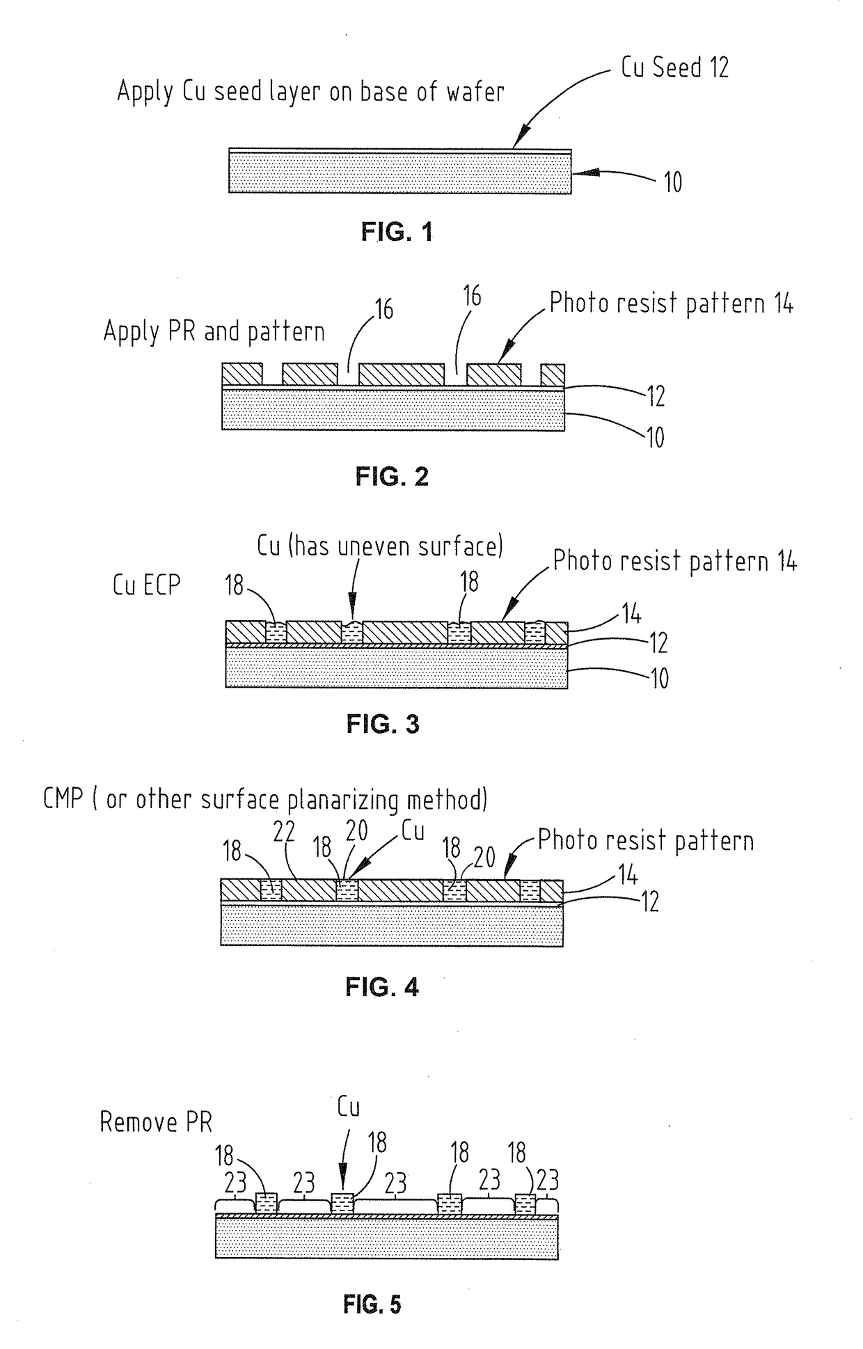
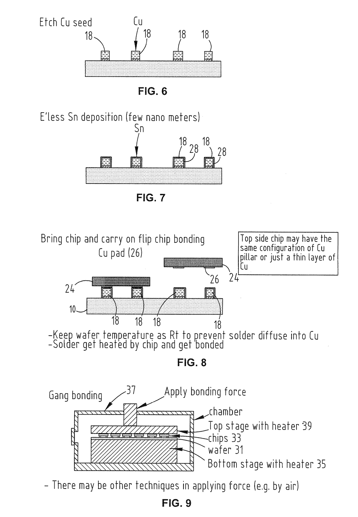
[0051]In a first embodiment, as shown in FIG. 6, bonding material, presently tin (Sn) solder 28, is deposited onto the posts 18. The solder 28 is deposited using electroless electroplating, though other techniques may be used. Similarly, another low melting point metal may be used in place of Sn.

[0052]The bonding material 28 is deposited in a thickness no greater than the surface roughness height of the planarized contact surface 20. While the surface height roughness will typically be less than 20 nm, even for rougher surfaces it is desirable that the bonding material thickness remain less than 1 micron. This reduces the likelihood that permanent bonding will be achieved using an intermetallic compound comprising the bonding material.

[0053]After application of the bonding material, the posts 18 are temporarily bonded to the contacts 26 using the bonding material to stabilize a position of the chip relative to the wafer 10 for permanent diffusion bonding of the chip to the wafer 10....

second embodiment

[0065]In a second embodiment, after regions of the Cu seed layer have been etched to complete formation of the posts, an electroless solvent is used to temporarily bond the chip to the wafer.

[0066]With reference to FIGS. 12(a), 12(b) and 12(c), to deposit the solvent onto the contacts 38 of a chip 40, a solvent bath or tray 50 containing electroless solvent is positioned between chip pick up and bonding in the flip chip bonder. During temporary bonding, the flip chip bonder picks up the chip 40 (see FIG. 12(a)) and dips it in the electroless solvent bath 50 (see FIG. 12(b)) to coat the contacts 38 (e.g. pads or posts) with solvent 41. While the solvent is wet the chip 40 is brought into register with the wafer 42 (see FIG. 12(c)). By contacting the chip 40 to the wafer 42, and ideally pressing the chip 40 to the wafer 42, solvent from the contacts 38 of the chip 40 flows onto, and coats, the contacts 44 of the wafer 42. In this manner the solvent fills between the contact surfaces 4...


PUM


Abstract

A method for chip on wafer bonding is provided. The method includes the formation of a plurality of posts on at least one of a chip and a wafer, and a like plurality of contacts on the other of the chip and the wafer. After formation, a contact surface of each post is planarized, the respective planarized contact surface having a surface roughness height. A bonding material is then applied to at least one of the chip in a thickness no greater than the surface roughness height of the contact surface. The posts are then temporarily bonded to the contacts using the bonding material to stabilize a position of the chip relative to the wafer for permanent diffusion bonding of the chip to the wafer.

Description

TECHNICAL FIELD[0001]The present disclosure provides a method for bonding one or more chips to a wafer.BACKGROUND ART[0002]Using conventional methodologies, a chip on wafer (CoW) bonding process involves the formation of copper (Cu) pillars on either the chip or the wafer, or both, before the chip is bonded to the wafer. If one of the chip and wafer does not include Cu pillars, it is instead provided with a Cu pad for bonding to the Cu pillars of the other of the chip and wafer. For simplicity, the following discussion will be limited to arrangements where there are pairs of opposing Cu pillars—i.e. the chip and wafer each have Cu pillars, with each Cu pillar of the chip aligning with a unique Cu pillar of the wafer—though the same discussion applies when bonding a Cu pillar to a Cu pad.[0003]Each Cu pillar consists of a Cu post and a solder cap. The solder cap is typically applied using electroplating, followed by a reflow process to round the cap. During bonding, the solder caps o...

Claims


Application Information

Patent Timeline
IPC IPC(8): H01L23/00H01L25/065H01L25/00
CPCH01L2224/13611H01L2224/13562H01L24/81H01L24/13H01L24/11H01L24/05H01L24/03H01L25/50H01L25/0657H01L2224/8182H01L2224/8181H01L2224/81022H01L2224/81099H01L2224/0345H01L2224/11462H01L2224/11464H01L2224/0401H01L2224/05147H01L2224/13026H01L2224/13147H01L2225/06513H01L2224/16225H01L2224/81H01L2224/11825H01L2224/0361H01L2224/05573H01L2224/05624H01L2224/05644H01L2224/05647H01L2224/1147H01L2224/11845H01L2224/119H01L2224/13023H01L2224/81097H01L2224/81192H01L2224/81193H01L2224/81203H01L2224/8183H01L2224/81986H01L2224/94H01L2224/97H01L2924/3841H01L2224/8109H01L2224/03622H01L2224/1184H01L2224/81805H01L2924/00014H01L2224/11H01L2224/03H01L2924/014H01L2224/9205
Inventor WICKRAMANAYAKA, SUNILXIE, LINGAW, JERRY JIE LI
Owner AGENCY FOR SCI TECH & RES
Why Eureka
Try Eureka