Solder bonded body, method of producing solder bonded body, element, photovoltaic cell, method of producing element and method of producing photovoltaic cell

a technology of solder bonded body and solder bonded body, which is applied in the direction of solventing apparatus, manufacturing tools, transportation and packaging, etc., can solve the problems of increased wiring resistance and contact resistance of surface electrodes, difficulty in achieving bonding between solder and the body to be bonded, and solder requires the above-described ultrasonic vibration

Inactive Publication Date: 2013-02-21
HITACHI CHEM CO LTD
View PDF0 Cites 23 Cited by
  • Summary
  • Abstract
  • Description
  • Claims
  • Application Information

AI Technical Summary

Benefits of technology

[0014]The first embodiment of the present invention is a solder bonded body, including: an oxide body to be bonded having an oxide layer on a surface thereof; and a solder layer bonded to the oxide layer, the solder layer having a zinc content of 1% by mass or less and being formed from an alloy containing at least two metals selected from the group consisting of tin, copper, silver, bismuth, lead, aluminum, titanium and silicon and having a melting point of lower than 450° C.

Problems solved by technology

However, in cases where the surfaces of the solder and body to be bonded are covered with an oxide of, for example, a surface oxide film used for the purposes of preventing natural oxidation in the air and providing surface protection, so-called “solder wettability” is poor and the solder and the body to be bonded do not come into direct contact with each other, so that diffusion of metal atoms does not occur, making it difficult to achieve bonding between the solder and the body to be bonded.
However, a flux residue, a residue of a halogen-based flux or the like, having residual activity, promotes the corrosion of the solder and the body to be bonded; therefore, it is required to remove such flux residues by washing after bonding treatment of the solder and the body to be bonded.
Further, this solder requires the above-described ultrasonic vibration at the time of soldering.
In this method, however, the above-described surface-coating process needs to be performed prior to bonding a solder, and in cases where the metal to be coated is easily corroded by the solder, it is required to strictly control the selection of applicable solder and the soldering conditions.
Therefore, when an attempt is made to bond the surface electrode with a wiring member such as a tab wire with a solder, the oxide film on the surface electrode may cause the above-described problems, resulting in an increase in the wiring resistance and contact resistance of the surface electrode.
This leads to voltage loss, which is relevant to conversion efficiency.

Method used


Image

  • Solder bonded body, method of producing solder bonded body, element, photovoltaic cell, method of producing element and method of producing photovoltaic cell
  • Solder bonded body, method of producing solder bonded body, element, photovoltaic cell, method of producing element and method of producing photovoltaic cell
  • Solder bonded body, method of producing solder bonded body, element, photovoltaic cell, method of producing element and method of producing photovoltaic cell

Examples


example 12

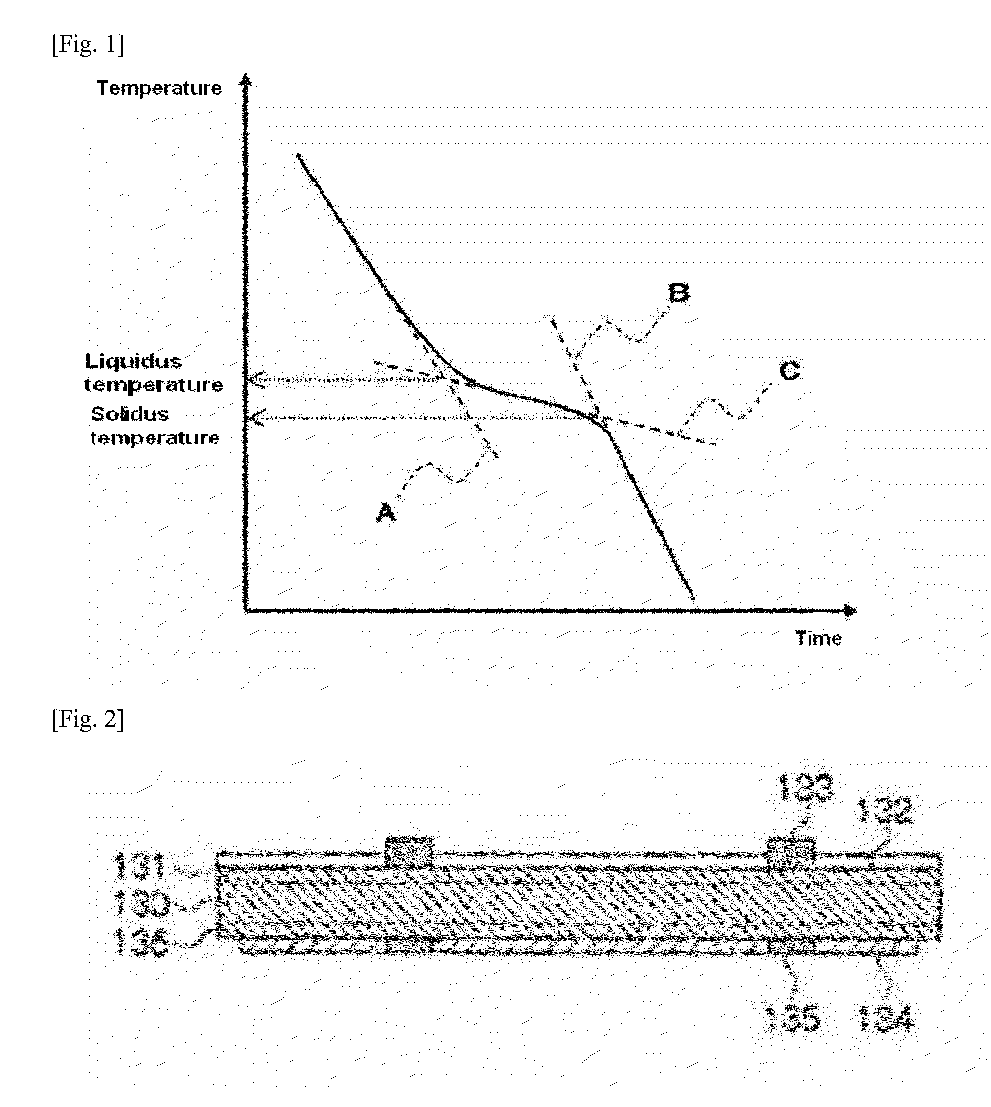
[0247]A solder 12 was prepared in the same manner as in Example 1 except that the bar solder and the plate lead were changed to a tin flat bar (manufactured by E-Material Inc.) and chipped bismuth (manufactured by E-Material Inc.) and that the solder composition was changed from 10 parts of tin and 90 parts of lead to 42 parts of tin and 58 parts of bismuth. Then, the bonding temperature and the bonding property were evaluated in the same manner as described in the above except that the thus obtained solder 12 was used. Further, as a result of examining the cooling curve of the solder 12, the liquidus temperature and the solidus temperature were found to be 141° C. and 139° C., respectively. The results are shown in Table 5.

example 13

[0248]A solder 13 was prepared in the same manner as in Example 12 except that a pure silver round wire (manufactured by Nitto Kagaku Co., Ltd.) was further used to change the solder composition from 42 parts of tin and 58 parts of bismuth to 42 parts of tin, 57 parts of bismuth and 1 part of silver. Then, the bonding temperature and the bonding property were evaluated in the same manner as described in the above except that the thus obtained solder 13 was used. Further, as a result of examining the cooling curve of the solder 13, the liquidus temperature and the solidus temperature were found to be 140° C. and 138° C., respectively. The results are shown in Table 5.

example 14

[0249]A solder 14 was prepared in the same manner as in Example 12 except that the solder composition was changed from 42 parts of tin and 58 parts of bismuth to 61 parts of tin and 39 parts of bismuth. Then, the bonding temperature and the bonding property were evaluated in the same manner as described in the above except that the thus obtained solder 14 was used. Further, as a result of examining the cooling curve of the solder 14, the liquidus temperature and the solidus temperature were found to be 177° C. and 138° C., respectively. The results are shown in Table 6.


PUM

PropertyMeasurementUnit
melting pointaaaaaaaaaa
solidus temperatureaaaaaaaaaa
temperatureaaaaaaaaaa

Abstract

The solder bonded body according to the present invention contains: an oxide body to be bonded having an oxide layer on the surface thereof; and a solder layer bonded to the oxide layer, which the solder layer is formed by an alloy containing at least two metals selected from the group consisting of tin, copper, silver, bismuth, lead, aluminum, titanium and silicon and having a melting point of lower than 450° C. and has a zinc content of 1% by mass or less.

Description

CROSS-REFERENCE TO RELATED APPLICATIONS[0001]This application claims priority under 35 U.S.C. 119(e) form Provisional U.S. Patent Application No. 61 / 522,830, filed Aug. 12, 2011, and Japanese Patent Applications Nos. 2011-176982 filed Aug. 12, 2011 and 2011-263043 filed Nov. 30, 2011, the disclosure of which is incorporated by reference herein.BACKGROUND OF THE INVENTION[0002]1. Field of the Invention[0003]The present invention relates to a solder bonded body, a method of producing the solder bonded body, an element, a photovoltaic cell, a method of producing the element and a method of producing the photovoltaic cell.[0004]2. Description of the Related Art[0005]Generally, solders are broadly classified as lead-containing solders and lead-free solders. In general, it is thought that, when a solder is brought into contact with a body to be bonded at a temperature of not lower than the melting point of the solder, metal atoms are diffused between the solder and the body to be bonded t...

Claims


Application Information

Patent Timeline
Patent Type & Authority Applications(United States)
IPC IPC(8): H01L31/0224H01L23/485B32B17/06B32B18/00B23K1/20B32B15/04
CPCB23K35/262B23K35/268B23K1/0016B23K1/203B23K2201/40Y02E10/50H01L2924/0002H01L31/022425H01L31/022441H01L2924/00B23K2101/40Y10T428/31678Y02E10/547
Inventor KURIHARA, YOSHIAKIYOSHIDA, MASATONOJIRI, TAKESHIADACHI, SHUICHIROKATO, TAKASHIKOKURATA, YASUSHI
Owner HITACHI CHEM CO LTD
Why Eureka
Try Eureka