Surface mounting device-type light emitting diode

Inactive Publication Date: 2008-01-31
SAMSUNG ELECTRONICS CO LTD
View PDF2 Cites 66 Cited by
  • Summary
  • Abstract
  • Description
  • Claims
  • Application Information

AI Technical Summary

Benefits of technology

[0015]An advantage of the present invention is that it provides an SMD-type LED in which a phosphor-mixed layer is reduced in thickness such that the reduction in energy of light passing through the phosphor-mixed layer is minimized. Then, it is possible to enhance overall light extraction efficiency of the LED.
[0016]Additional aspect and advantages of the present general inventive concept will be set forth in part in the description which follows and, in part, will be obvious from the description, or may be learned by practice of the general inventive concept.
[0017]According to an aspect of the invention, an SMD-type LED comprises a package housing one or more pairs of electrodes therein, the package having a predetermined space in the center thereof and a light-emission window which is opened so that light is emitted through the light-emission window; a lens formed on the package so as to cover the light-emission window; an LED chip formed o

Problems solved by technology

As a result, light extraction efficiency decreases.
Therefore, a consumed

Method used


Image

  • Surface mounting device-type light emitting diode
  • Surface mounting device-type light emitting diode
  • Surface mounting device-type light emitting diode

Examples


Example

First Embodiment

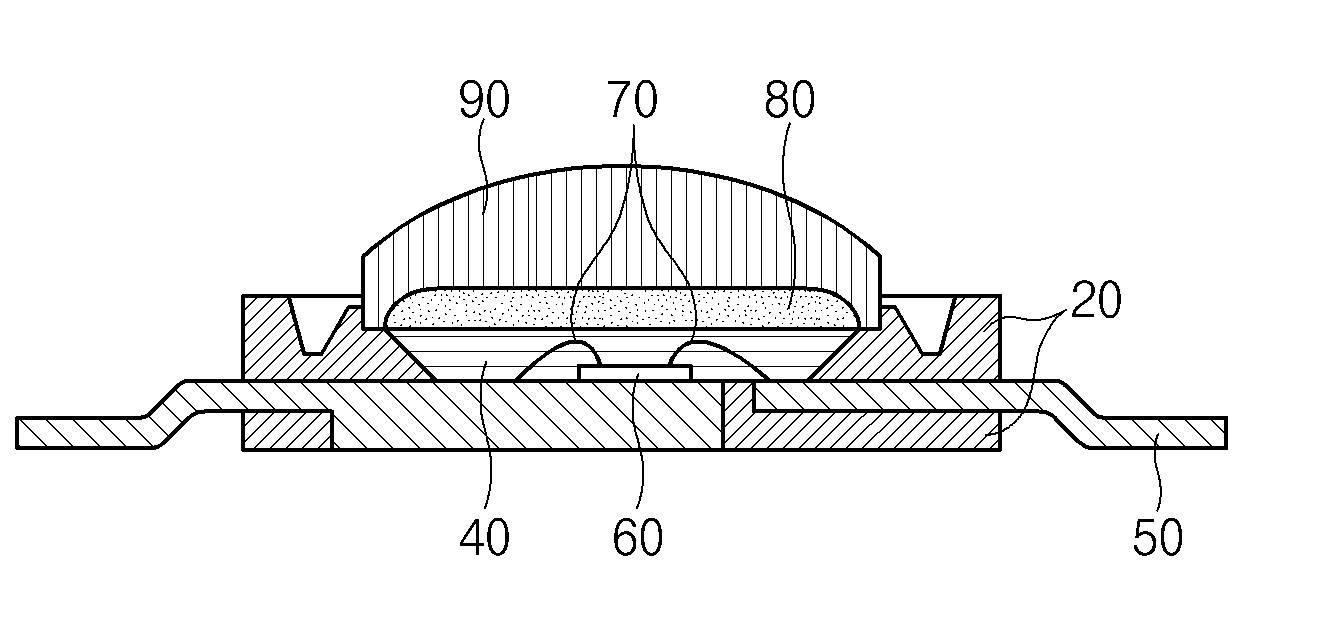
[0033]Referring to FIG. 3, an SMD-type LED according to a first embodiment of the invention will be described in detail.

[0034]FIG. 3 is a sectional view of the SMD-type LED according to the first embodiment of the invention.

[0035]Referring to FIG. 3, the SMD-type LED according to the first embodiment of the invention has a package 20 having a cavity formed in the central inner portion thereof. The package 20 has an emission window formed on a predetermined surface thereof such that light is easily emitted through the emission window. On the package 20, a lens 90 is positioned.

[0036]The surface of the lens 90, which is adjacent to the emission window, is formed to have a groove which is concave toward the lens 90. The concave groove of the lens 90 serves to define a formation region of a phosphor-mixed layer to be described below.

[0037]In this embodiment, it is shown that the concave groove of the lens 90 is formed with a curved surface. Without being limited thereto,...

Example

Second Embodiment

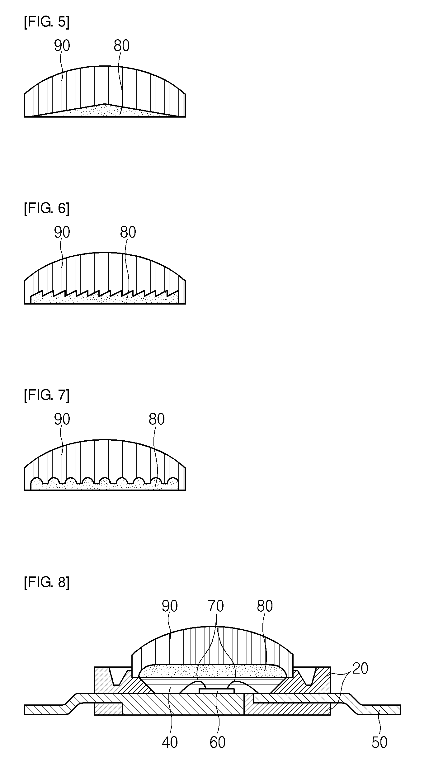
[0050]Next, a second embodiment of the invention will be described with reference to FIG. 8. However, the descriptions of the same components as those of the first embodiment will be omitted.

[0051]FIG. 8 is a sectional view illustrating the structure of an SMD-type LED according to the second embodiment of the invention.

[0052]As shown in FIG. 8, the SMD-type LED according to the second embodiment has almost the same construction as the SMD-type LED according to the first embodiment. However, the SMD-type LED according to the second embodiment is different from that of the first embodiment only in that liquid resin 40 is filled inside the package 20 having the LED chip 60 mounted therein.

[0053]Since the SMD-type LED according to the second embodiment also has the phosphor-mixed layer 80 formed on the surface of the lens 90 adjacent to the light-emission window of the package 20, it is possible to obtain the same operation and effect as the first embodiment. Further, ...


PUM


Abstract

A surface mounting device-type light emitting diode (SMD-type LED) comprises a package housing one or more pairs of electrodes therein, the package having a predetermined space in the center thereof and a light-emission window which is opened so that light is emitted through the light-emission window; a lens formed on the package so as to cover the light-emission window; an LED chip formed on an electrode inside the package; a wire for electrically connecting the LED chip and the electrode; and a phosphor-mixed layer formed on the surface of the lens adjacent to the light-emission window.

Description

CROSS-REFERENCE TO RELATED APPLICATIONS[0001]This application claims the benefit of Korean Patent Application No. 10-2006-0070622 filed with the Korean Intellectual Property Office on Jul. 27, 2006, the disclosure of which is incorporated herein by reference.BACKGROUND OF THE INVENTION[0002]1. Field of the Invention[0003]The present invention relates to a surface mounting device-type light emitting diode (hereinafter, referred to as an SMD-type LED) which maximizes efficiency of phosphor such that extraction efficiency of light to be emitted into a lens can be enhanced.[0004]2. Description of the Related Art[0005]Generally, a light emitting diode (hereinafter, referred to as ‘LED’) has light sources provided by varying compound semiconductor materials such as GaAs, AlGaAs, GaN, InGaInP and the like, thereby implementing various colors of light.[0006]Recently, as the semiconductor technology rapidly develops, the production of LEDs with high luminance and high quality has become poss...

Claims


Application Information

Patent Timeline
IPC IPC(8): H01L33/00H01L33/50H01L33/56H01L33/58H01L33/60H01L33/62
CPCH01L33/507H01L33/58H01L2224/48091H01L2224/48247H01L2924/00014
Inventor CHAE, JOON-SEOKBAEK, JONG HWAN
Owner SAMSUNG ELECTRONICS CO LTD
Why Eureka
Try Eureka