Method for depositing and curing low-k films for gapfill and conformal film applications

a technology of conformal film and low-k film, which is applied in the direction of coating, chemical vapor deposition coating, coating process, etc., can solve the problems of low-moisture oxide film k-value, low k-value, werr, etc., and achieves the effect of reducing the k-value of low-moisture oxide film, and reducing the k-value of low-mois-

Active Publication Date: 2008-01-31
APPLIED MATERIALS INC
View PDF99 Cites 418 Cited by
  • Summary
  • Abstract
  • Description
  • Claims
  • Application Information

AI Technical Summary

Benefits of technology

[0007] Embodiments of the invention include methods of making a silicon oxide layer on a substrate. The methods may include forming the silicon oxide layer on the substrate in a reaction chamber by reacting an atomic oxygen precursor and a silicon precursor and depositing reaction products on the substrate. The atomic oxygen precursor may be generated outside the reaction chamber. The methods may also include heating the silicon oxide layer at a temperature of about 600° C. or less, and exposing the silicon oxide layer to an induced coupled plasma.

Problems solved by technology

Unfortunately, there are few (if any) starting materials that combine all these qualities in a simple deposition.
On the other hand, depositions of low-moisture oxide films typically have lower k-values and WERRs, but are also more prone to forming gaps and seams due to their reduced flowability.
However, higher temperature anneals have to be balanced against thermal budget constraints in the fabrication process.
In some instances, thermal budgets that low can make thermal annealing impractical due to the long anneal times.
Charged particles from the plasma strike the oxide film and cause the disruption of silanol bonds and removal of water vapor.
The highly energetic plasma particles can also disrupt carbon-silicon and carbon-carbon bonds in the oxide film.
However, for low-k oxide films that incorporate carbon to lower the dielectric constant of the material, carbon removal by the plasma can damage the film by increasing its k-value.

Method used


Image

  • Method for depositing and curing low-k films for gapfill and conformal film applications
  • Method for depositing and curing low-k films for gapfill and conformal film applications
  • Method for depositing and curing low-k films for gapfill and conformal film applications

Examples


Embodiment Construction

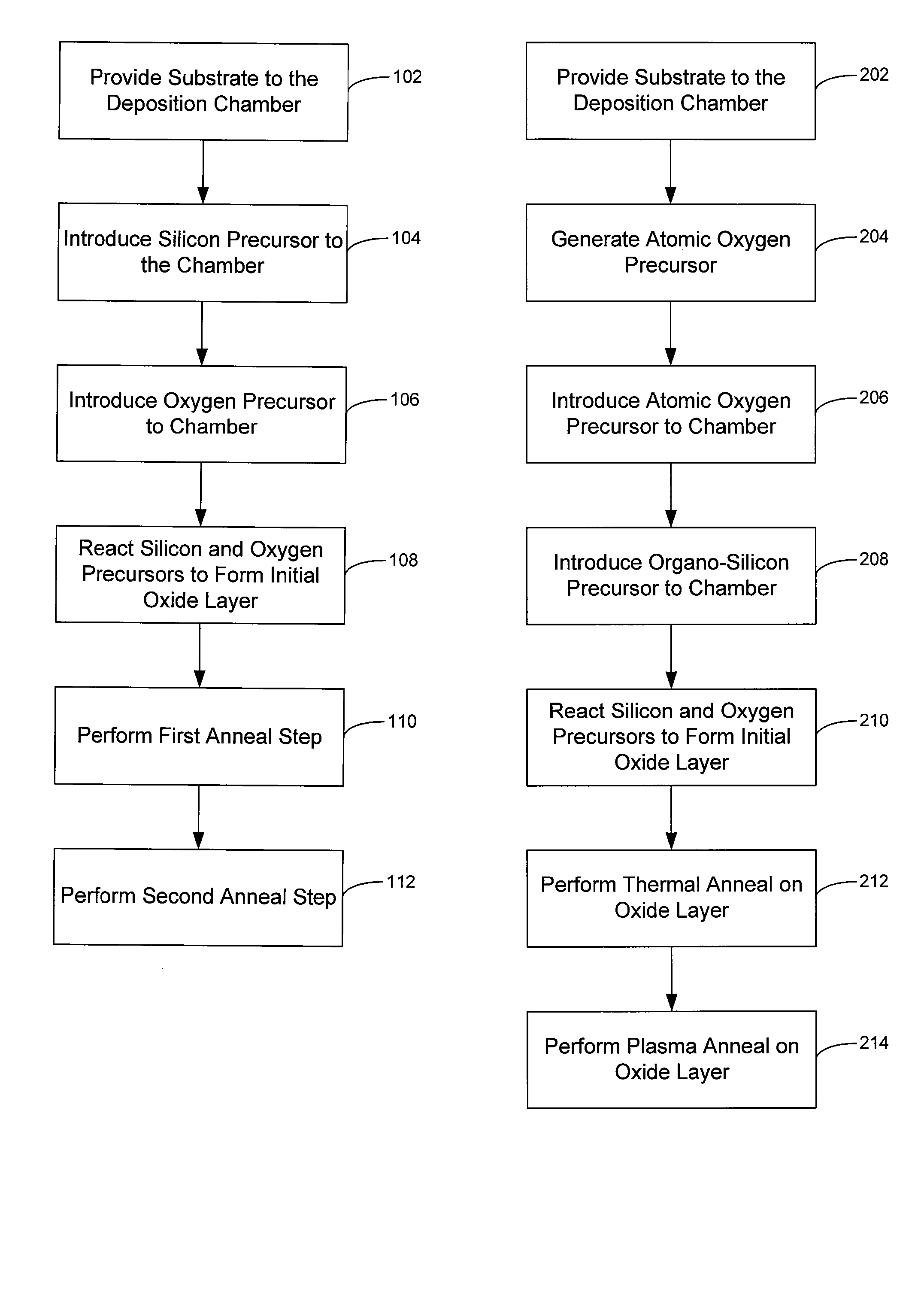
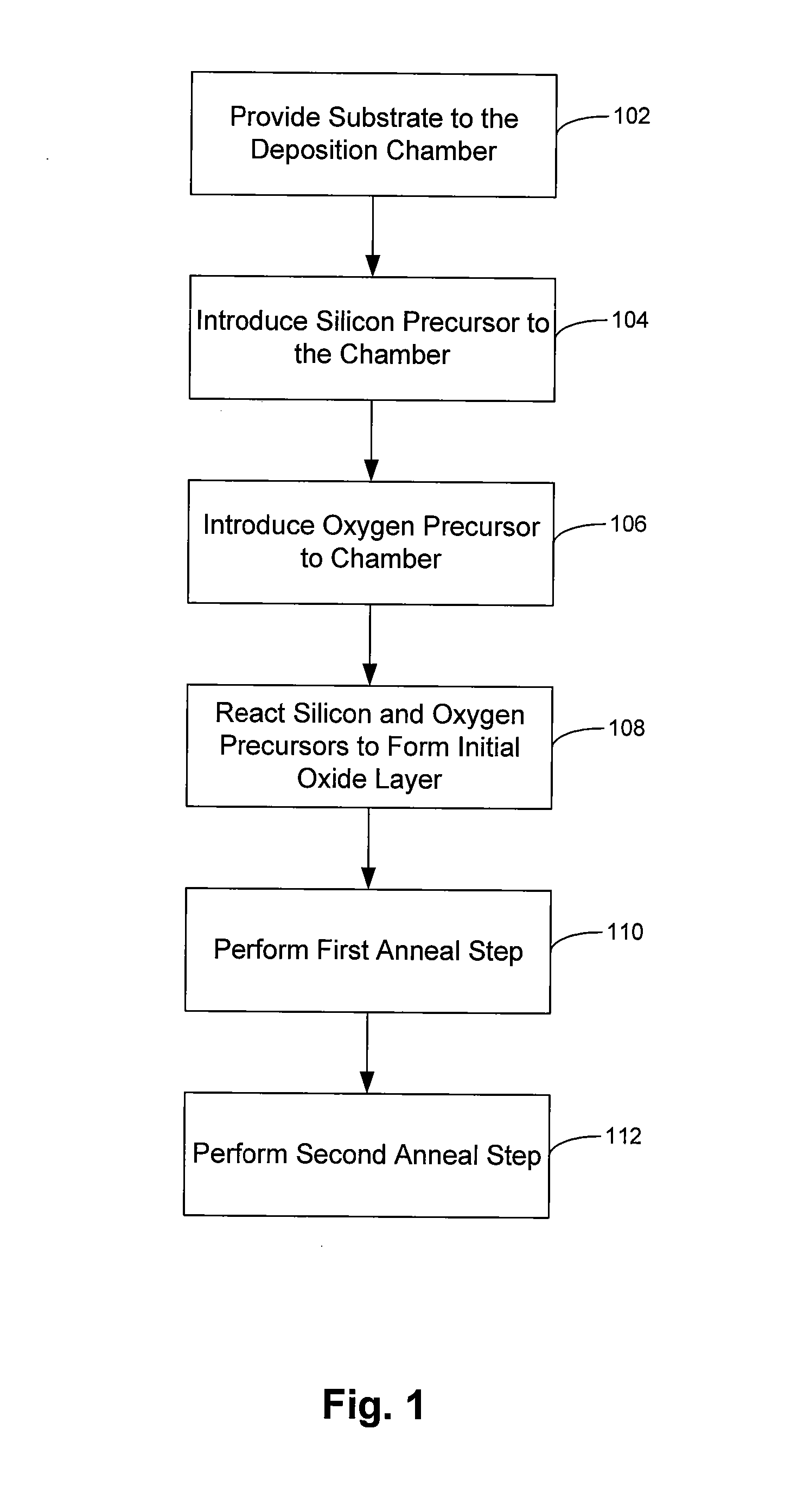
[0020] Systems and methods are described for multistage anneals of silicon oxide layers. The multistage anneal permits the efficient removal of moisture and silanol groups from an oxide layer without requiring high temperatures (e.g., temperatures in excess of 600° C.). The multistage anneal may include a first stage anneal that increases the hardness of the layer and removes a portion of the moisture and / or hydroxyl groups, and a second stage anneal that removes most (if not all) the remaining moisture and hydroxyl groups to produce a hard oxide layer (e.g., greater than 1 GPa) with good dielectric characteristics (e.g., k-value less than 3).

[0021] The multistage anneals can transform an initially deposited soft oxide film into a high-quality, low-k dielectric layer without requiring high temperatures or long anneal times (e.g., greater than 60 minutes). For carbon containing low-k oxide layers, the first stage of the anneal hardens the soft film to the point that a subsequent ann...


PUM

PropertyMeasurementUnit
temperatureaaaaaaaaaa
pressureaaaaaaaaaa

Abstract

Methods of making a silicon oxide layer on a substrate are described. The methods may include forming the silicon oxide layer on the substrate in a reaction chamber by reacting an atomic oxygen precursor and a silicon precursor and depositing reaction products on the substrate. The atomic oxygen precursor is generated outside the reaction chamber. The methods also include heating the silicon oxide layer at a temperature of about 600° C. or less, and exposing the silicon oxide layer to an induced coupled plasma. Additional methods are described where the deposited silicon oxide layer is cured by exposing the layer to ultra-violet light, and also exposing the layer to an induced coupled plasma.

Description

CROSS-REFERENCES TO RELATED APPLICATIONS [0001] This application claims the benefit of U.S. Provisional Application No. 60 / 803,489 by Munro et al, filed May 30, 2006 and titled “A METHOD FOR DEPOSITING AND CURING LOW-K FILMS FOR GAPFILL AND CONFORMAL FILM APPLICATIONS”. This application is also related to co-assigned U.S. Provisional App. No. 60 / 803,493, by Ingle et al, filed May 30, 2006 and titled “CHEMICAL VAPOR DEPOSITION OF HIGH QUALITY FLOW-LIKE SILICON DIOXIDE USING A SILICON CONTAINING PRECURSOR AND ATOMIC OXYGEN”. This application is also related to U.S. Provisional Application No. 60 / 803,481, by Chen et al, filed May 30, 2006 and titled “A NOVEL DEPOSITION-PLASMA CURE CYCLE PROCESS TO ENHANCE FILM QUALITY OF SILICON DIOXIDE”. In addition, this application is related to U.S. Provisional Application No. 60 / 803,499 by Lubomirsky, filed May 30, 2006 and titled “PROCESS CHAMBER FOR DIELECTRIC GAPFILL”. The entire contents of the priority U.S. Provisional patent application and ...

Claims


Application Information

Patent Timeline
Patent Type & Authority Applications(United States)
IPC IPC(8): H01L21/31
CPCC23C16/401C23C16/452C23C16/56H01L21/31633H01L21/02164H01L21/02274H01L21/3105H01L21/02126H01L21/205
Inventor MUNRO, JEFFREY C.NEMANI, SRINIVAS D.
Owner APPLIED MATERIALS INC
Why Eureka
Try Eureka