Precision fabricated silicon mold

a technology of silicon molds and molds, applied in the field of molds or forms, can solve the problem of limiting the size of interconnects that can be transferred

Inactive Publication Date: 2008-02-07
IBM CORP
View PDF23 Cites 5 Cited by
  • Summary
  • Abstract
  • Description
  • Claims
  • Application Information

AI Technical Summary

Benefits of technology

[0008]In view of the foregoing, an embodiment of the invention provides a reusable precision fabricated silicon mold comprising a mold made of silicon which comprises a desired pattern of physical features or cavities etched into the mold to transfer a patter on bumps to a semiconductor wafer (e.g., computer chip, semiconductor device, silicon on insulator device, etc.); an aperture etched into the mold adapted to allow gases to escape but does not to allow a conductive a...

Problems solved by technology

The materials used for these molds (i.e., masks) and the tooling techniques ava...

Method used


Image

  • Precision fabricated silicon mold
  • Precision fabricated silicon mold
  • Precision fabricated silicon mold

Examples


Embodiment Construction

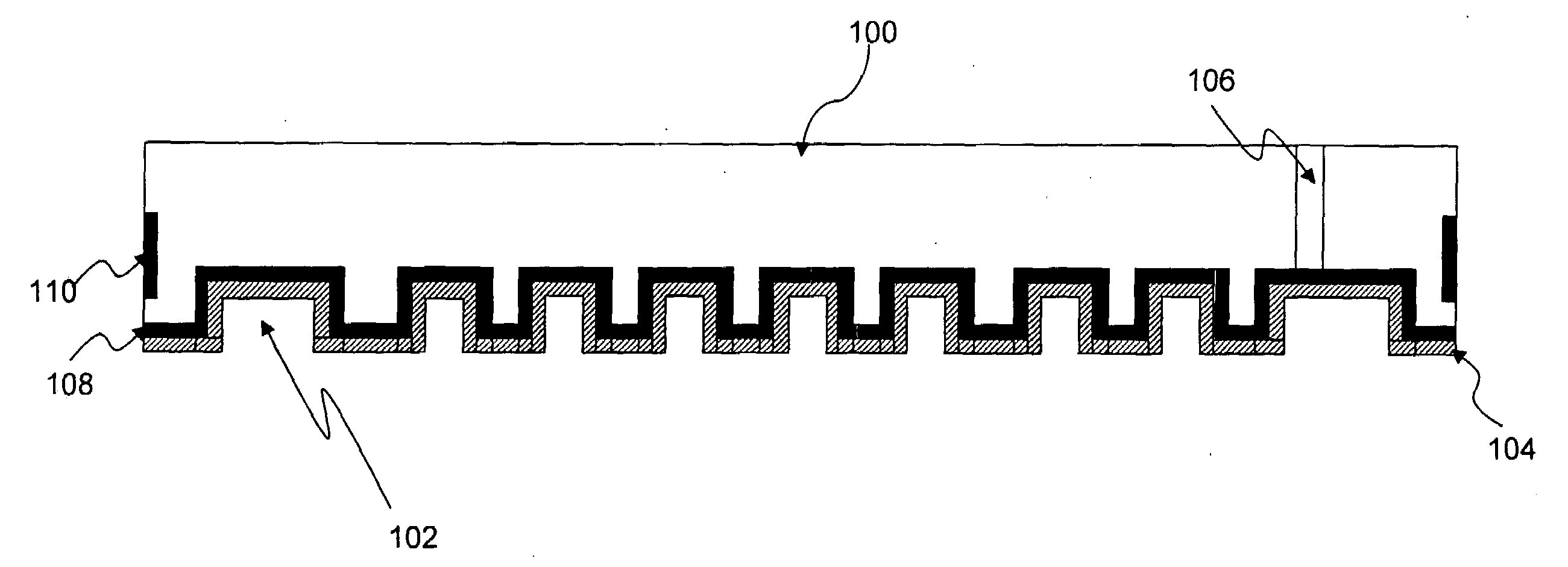
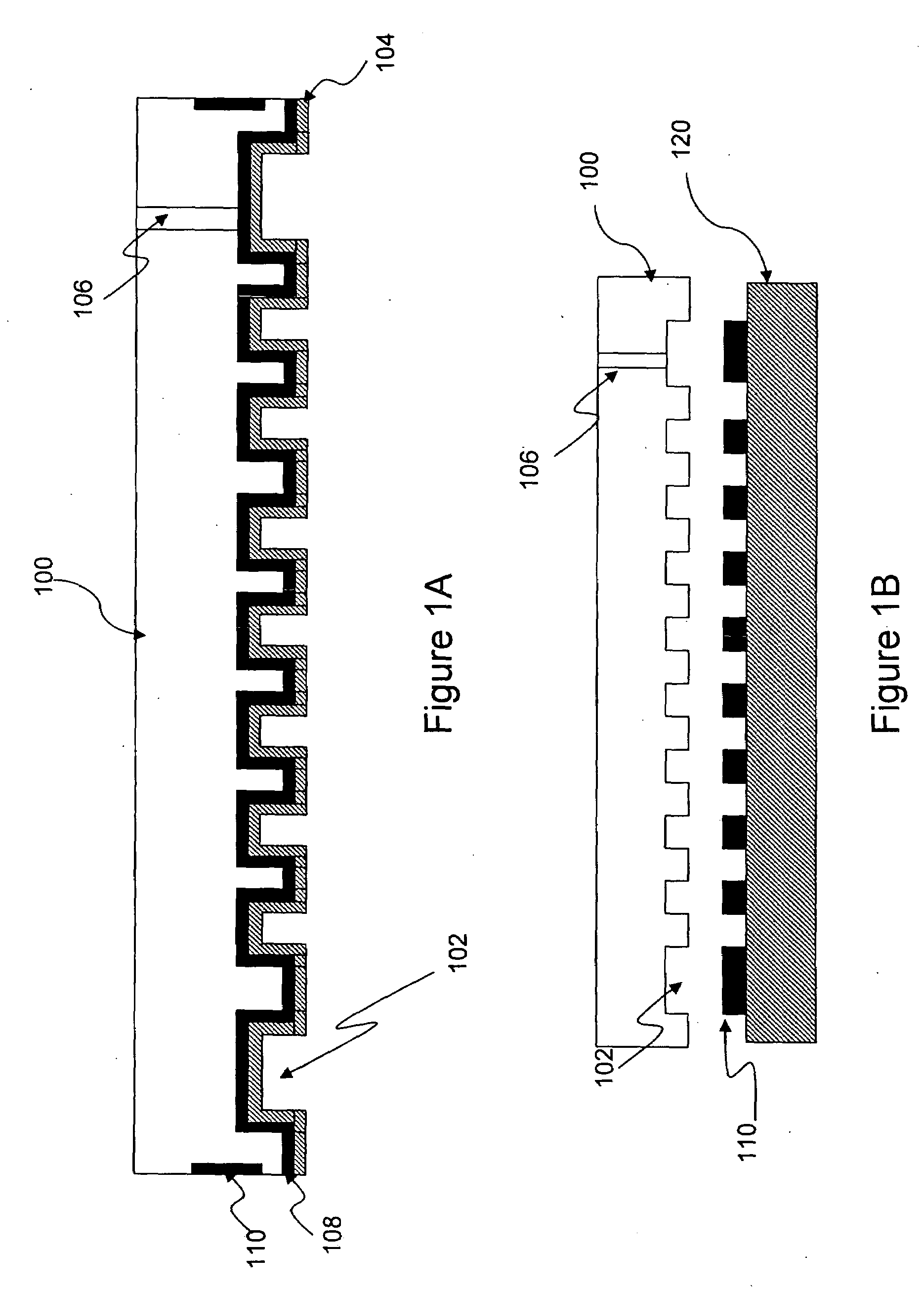
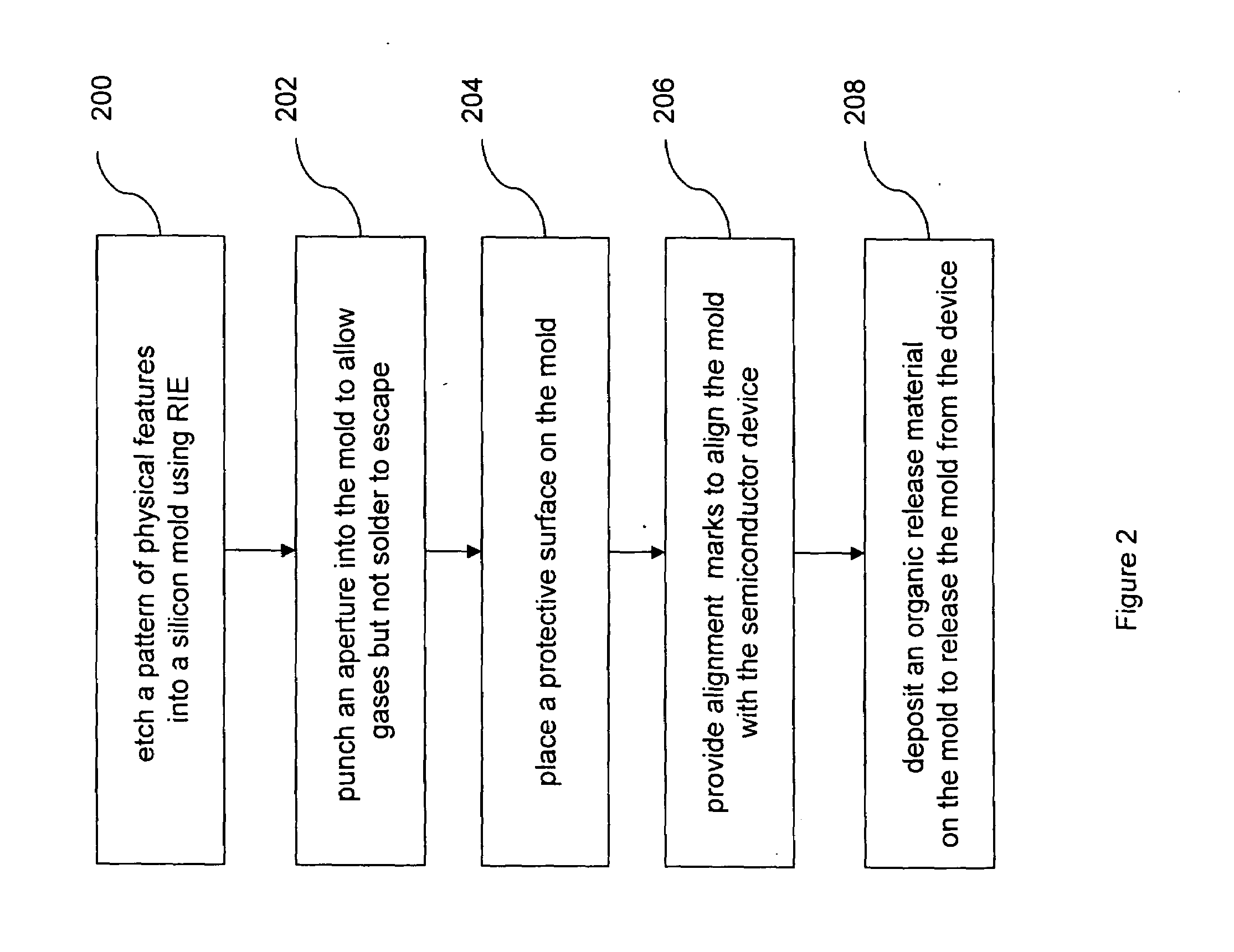
[0014]The embodiments of the invention and the various features and advantageous details thereof are explained more fully with reference to the non-limiting embodiments that are illustrated in the accompanying drawings and detailed in the following description. It should be noted that the features illustrated in the drawings are not necessarily drawn to scale. Descriptions of well-known components and processing techniques are omitted so as to not unnecessarily obscure the embodiments of the invention. The examples used herein are intended merely to facilitate an understanding of ways in which the embodiments of the invention may be practiced and to further enable those of skill in the art to practice the embodiments of the invention. Accordingly, the examples should not be construed as limiting the scope of the embodiments of the invention.

[0015]As mentioned, there remains a need for decreased interconnect size to allow for higher interconnect density on a chip as well as a minimiz...


PUM

PropertyMeasurementUnit
Temperatureaaaaaaaaaa
Sizeaaaaaaaaaa

Abstract

The invention provides a reusable precision fabricated silicon mold comprising a mold made of silicon which comprises a desired pattern of physical features cavities etched into the mold to transfer a patter on bumps to a semiconductor wafer, e.g., computer chip, semiconductor device, silicon on insulator device, etc.; an aperture etched into the mold adapted to allow gases to escape but does not to allow a solder to escape during the process of transferring solder bumps to a chip; a protective oxide or nitride on the mold; alignment marks adapted to properly align the mold with a semiconductor wafer; an organic release material on the mold adapted to release the mold from the semiconductor wafer, wherein the mold precisely defines a conductive adhesive material volume for interconnects on the semiconductor wafer.

Description

BACKGROUND[0001]1. Field of the Invention[0002]The embodiments of the invention generally relate to a mold or form for making interconnects on an electronic device, and, more particularly, to a precision reusable silicon mold / form that minimizes defect density on an electronic device.[0003]2. Description of the Related Art[0004]As electronic devices such as mobile phones, portable digital assistants, and computers get smaller in size, yet have increased functionality, more interconnects on semiconductor devices in order to achieve the increased functionality in these devices become desirable. Present methods for transferring patterns of solder bumps onto to electronic devices (e.g., semiconductor wafers, silicon on insulator wafers, etc.) to provide for interconnects or vias on the device include using molds to transfer the solder (e.g., conductive adhesive) to the semiconductor wafer. The materials used for these molds (i.e., masks) and the tooling techniques available for making t...

Claims


Application Information

Patent Timeline
IPC IPC(8): B29C33/56
CPCB29C33/405B29K2083/00B29C33/60B29C33/56
Inventor GRUBER, PETER A.KNICKERBOCKER, JOHN U.
Owner IBM CORP
Why Eureka
Try Eureka