Manufacturing method of high aspect ratio micro structure of novel carbon-carbon nano tube composite material

A technology of carbon nanotubes and composite materials, which is applied in the field of preparation and molding of microstructures, can solve the problem that carbon or carbon nanotubes cannot be obtained cheaply and efficiently, and achieve good application prospects, good mechanical properties, and high resonance frequency.

Inactive Publication Date: 2015-05-13
WUHAN UNIV OF TECH
View PDF5 Cites 3 Cited by
  • Summary
  • Abstract
  • Description
  • Claims
  • Application Information

AI Technical Summary

Problems solved by technology

The existing mainstream ICP-RIE (Inductively Coupled Plasma Reactive Ion Etching) technology for making high aspect ratio microstructures and LIGA technology can be combined with micro injection molding technology to man

Method used


Image

  • Manufacturing method of high aspect ratio micro structure of novel carbon-carbon nano tube composite material
  • Manufacturing method of high aspect ratio micro structure of novel carbon-carbon nano tube composite material

Examples


Embodiment 1

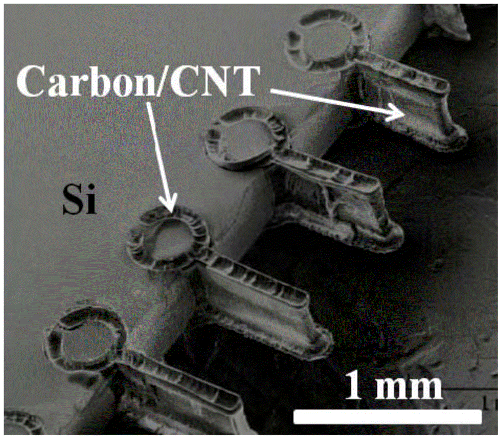
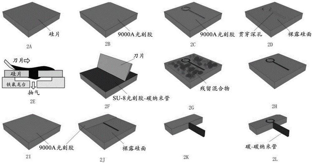
[0033] A method for making a micro-cantilever beam of a novel carbon-carbon nanotube composite material, comprising the following steps:

[0034] 1) Clean the wafer with a typical RCA cleaning process (see figure 2 A);

[0035] 2) Use 9000A photoresist to spin-coat glue on one surface of the silicon wafer described in 1), and the rotating speed is: the first step, 5s, 500rpm; the second step, 30s, 2500rpm (see figure 2 B);

[0036] 3) Using a mask with a cantilever beam geometry, perform photolithography on the silicon wafer that has been glued as described in step 2), and the exposure dose is 400mJ / cm 2 ;

[0037] 4) Immerse the silicon wafer described in step 3) in RD-6 developer solution, No. 1 deionized water, and No. 2 deionized water in sequence; the immersion and development time is: RD-6 developer solution, 35s; No. 1 deionized water Water, 40s; No. 2 deionized water, 40s (see figure 2 C);

[0038] 5) carry out ICP-RIE deep etching to the sample with photoresi...

Embodiment 2

[0049] A method for making a micro-cantilever beam of a novel carbon-carbon nanotube composite material, comprising the following steps:

[0050] 1) Clean the silicon wafer with a typical RCA cleaning process;

[0051] 2) Use 9000A photoresist to spin-coat glue on one surface of the silicon wafer described in step 1), the speed is, the first step: 5s, 500rpm, the second step: 30s, 2500rpm;

[0052] 3) Using a reticle with a micro-cantilever geometry, perform photolithography on the silicon wafer that has been glued as described in step 2), and the exposure dose is 400mJ / cm 2 ;

[0053] 4) Immerse the silicon wafer described in step 3) in RD-6 developing solution, No. 1 deionized water, and No. 2 deionized water in sequence. Water, 40s, No. 2 deionized water, 40s;

[0054] 5) carry out ICP-RIE deep etching to the sample with photoresist pattern described in step 4), form the deep hole that runs through the silicon chip, obtain micro silicon mold;

[0055] 6) Carry out 1200 ...

Embodiment 3

[0066] A method for making a micro-cantilever beam of a novel carbon-carbon nanotube composite material, comprising the following steps:

[0067] 1) Clean the silicon wafer with a typical RCA cleaning process;

[0068] 2) Use 9000A photoresist to spin coat glue on one surface of the silicon wafer described in step 1), the speed is: the first step, 5s, 500rpm; the second step, 30s, 2500rpm;

[0069] 3) Using a mask with a cantilever beam geometry, perform photolithography on the silicon wafer that has been glued as described in step 2), and the exposure dose is 400mJ / cm 2 ;

[0070] 4) Dip the silicon wafer described in step 3) into RD-6 developer, No. 1 deionized water, and No. 2 deionized water in sequence. Soaking and developing time: RD-6 developer, 35s; No. 1 deionized water, 40s; No. 2 deionized water, 40s;

[0071] 5) carry out ICP-RIE deep etching to the sample with photoresist pattern described in step 4), form the deep hole that runs through the silicon chip, obtai...


PUM

PropertyMeasurementUnit
Thicknessaaaaaaaaaa
Radiusaaaaaaaaaa
Lengthaaaaaaaaaa

Abstract

The invention provides a manufacturing method of a high aspect ratio micro structure of a novel carbon-carbon nano tube composite material. The manufacturing method comprises the following steps of manufacturing a micro silicon mold and manufacturing the carbon-carbon nano tube composite material and the high aspect ratio micro structure, wherein the micro silicon mold is prepared by an ultraviolet photoetching and silicon deep etching technique; the novel carbon-carbon nano tube composite material is obtained by carbonizing a photoetching-carbon nano tube composite material obtained by mixing a multi-wall carbon nano tube and SU-8 photoresist; the high aspect ratio micro structure can be prepared in a micro silicon mold by a background vacuumizing method. According to the invention, relevant techniques in the field of semiconductors are fused; the technology is simple, and the relevant techniques are developed, and the manufacturing method can be applied to the large-scale production; the micro structure of the obtained carbon-carbon nano tube composite material has good mechanical property and relatively high chemical stability; the micro structure with the width range of 5-100 microns and the depth range of 200-500 microns can be obtained; the highest depth-to-width ratio can reach 100.

Description

technical field [0001] The invention relates to the intersection field of nanomaterials and micromachining technology, in particular to a method for preparing and forming a microstructure based on a novel carbon-carbon nanotube composite material with high aspect ratio. Background technique [0002] High aspect ratio microstructures are widely used in micro-mechanical fields such as micro-sensors, micro-energy hunters, and micro-drivers, and have extremely high application value. As a new type of material, carbon nanotubes have good theoretical mechanical properties and chemical stability, and are often incorporated into other materials to enhance mechanical properties. The existing mainstream ICP-RIE (Inductively Coupled Plasma Reactive Ion Etching) technology for making high aspect ratio microstructures and LIGA technology can be combined with micro injection molding technology to manufacture high aspect ratio microstructures made of metals, ceramics, silicon, polymers, et...

Claims


Application Information

Patent Timeline
IPC IPC(8): B81C99/00
Inventor 何亮麦立强杨枭周鹏熊彪
Owner WUHAN UNIV OF TECH
Why Eureka
Try Eureka