Structure and method for making high density mosfet circuits with different height contact lines

a high-density mosfet and contact line technology, applied in the direction of semiconductor devices, electrical apparatus, transistors, etc., can solve the problems of source and drain blockage, inconvenient integration into conventional processes, and inconvenient use of spacers, so as to reduce the height and thickness of spacers, the effect of easy integration into conventional processes

Inactive Publication Date: 2008-02-07
ELPIS TECH INC
View PDF26 Cites 6 Cited by
  • Summary
  • Abstract
  • Description
  • Claims
  • Application Information

AI Technical Summary

Benefits of technology

[0013] Accordingly, embodiments of the invention provide a structure and method for making high density MOSFET circuits with different height contact lines. Specifically, lower contact lines are used to reduce both spacer height and spacer thickness. This reduces the chance of spacers blocking via hole etching. Since spacers on polysilicon contact lines can block via contacts, the via contacts can be separated from the source / drain areas of the MOSFET circuit. For example, spacer blocking causes circuit opens in static random access memory (SRAM). This problem is intensified as SRAM areas continue to shrink. Therefore, the structure and method of embodiments of the invention provide a solution that is easy to integrate into conventional processes of MOSFET manufacturing.

Problems solved by technology

Despite its advantages, MOSFET circuits are susceptible to source and drain blockage due to aggressive scaling of semiconductor devices.
Specifically, the source and drain areas of MOSFET circuits are becoming increasingly smaller, which can lead to blockage of the source and drain areas by spacers.
However, spacers are not always useful and in some cases have disadvantages.
Spacers on the contact lines can increase the difficulty forming contact between the contact lines and the devices needed to contact.
Moreover, these undesirable spacers occupy space and then reduce density of ICs.
This increases the costs of manufacturing of ICs.

Method used


Image

  • Structure and method for making high density mosfet circuits with different height contact lines
  • Structure and method for making high density mosfet circuits with different height contact lines
  • Structure and method for making high density mosfet circuits with different height contact lines

Examples


Embodiment Construction

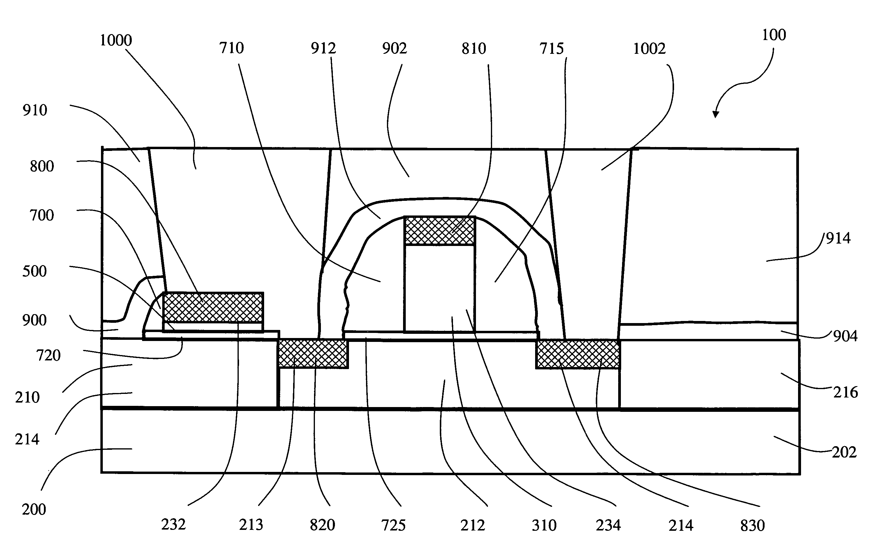
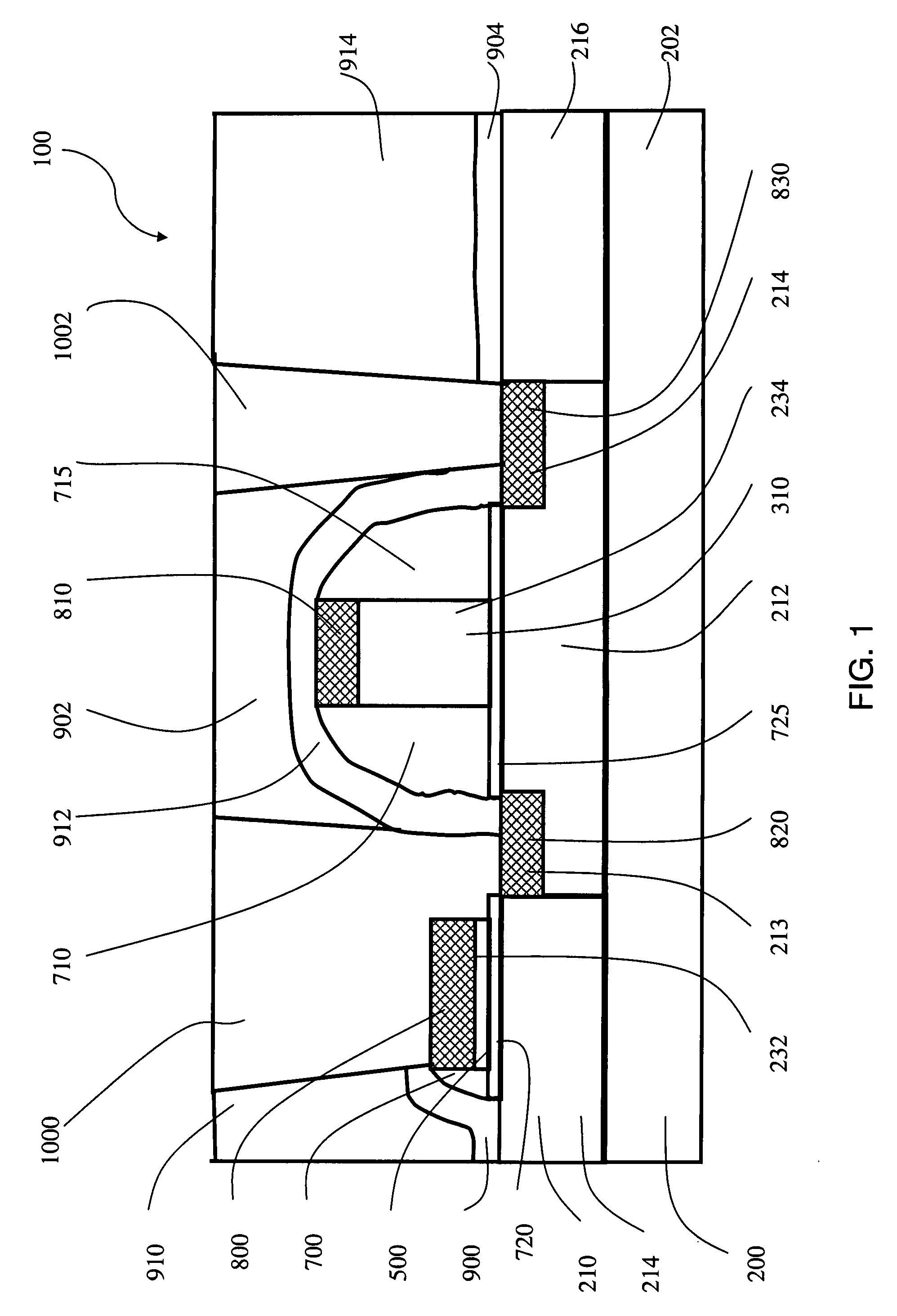
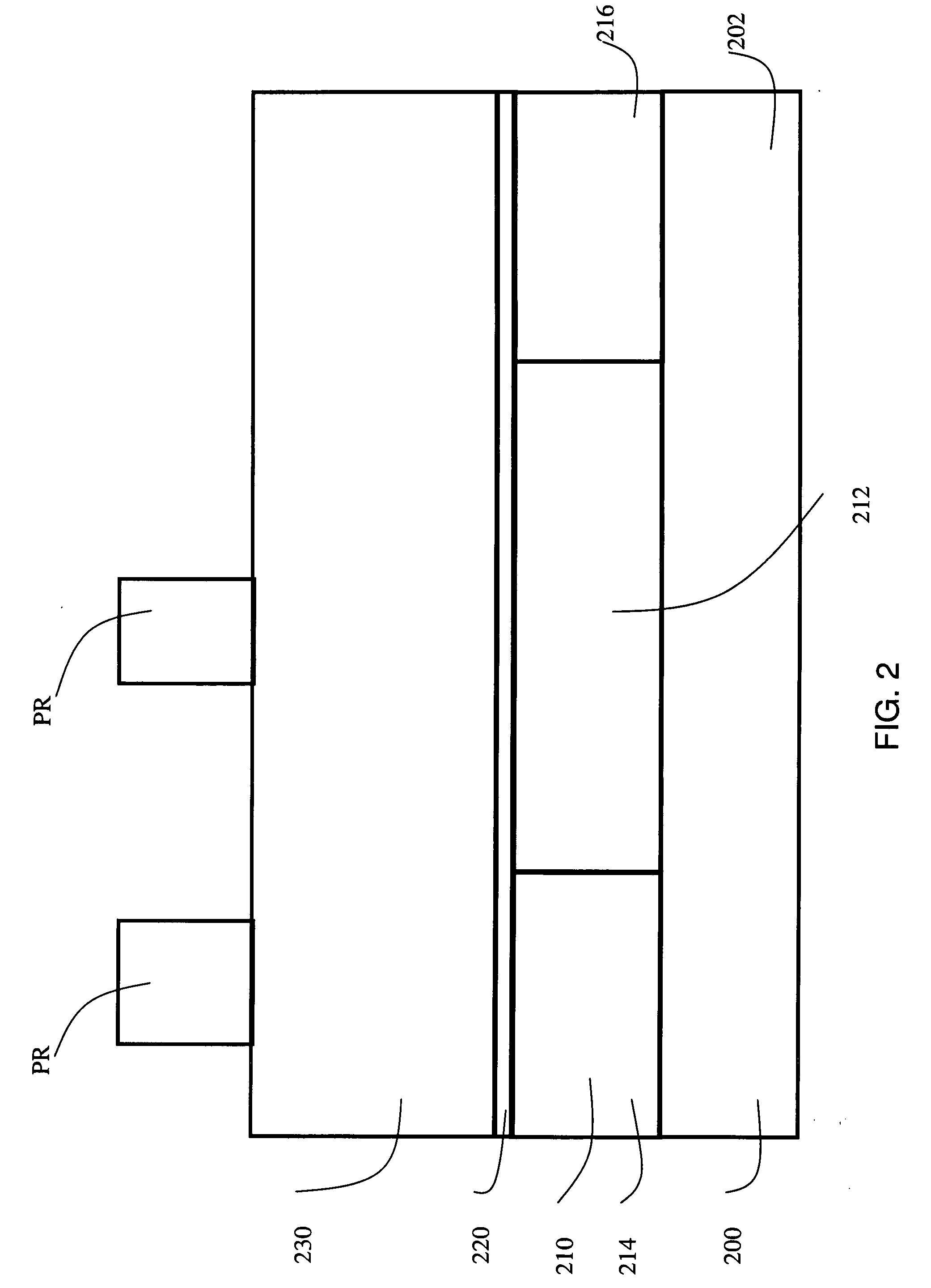
[0038] The embodiments of the invention and the various features and advantageous details thereof are explained more fully with reference to the non-limiting embodiments that are illustrated in the accompanying drawings and detailed in the following description. It should be noted that the features illustrated in the drawings are not necessarily drawn to scale. Descriptions of well-known components and processing techniques are omitted so as to not unnecessarily obscure the embodiments of the invention. The examples used herein are intended merely to facilitate an understanding of ways in which the embodiments of the invention may be practiced and to further enable those of skill in the art to practice the embodiments of the invention. Accordingly, the examples should not be construed as limiting the scope of the embodiments of the invention.

[0039] Embodiments of the invention provide a structure and method for making high density MOSFET circuits with different height contact lines...


PUM


Abstract

Embodiments herein present a structure, method, etc. for making high density MOSFET circuits with different height contact lines. The MOSFET circuits comprise a contact line, a first gate layer situated proximate the contact line, and at least one subsequent gate layer situated over the first gate layer. The contact line comprises a height that is less than a combined height of the first gate layer and the subsequent gate layer(s). The MOSFET circuits further comprise gate spacers situated proximate the gate layers and a single contact line spacer situated proximate the contact line. The gate spacers are taller and thicker than the contact line spacer.

Description

CROSS-REFERENCE TO RELATED APPLICATIONS [0001] This application is a continuation of U.S. application Ser. No. 11 / 306,707 filed Jan. 9, 2006, the complete disclosure of which, in its entirety, is herein incorporated by reference.BACKGROUND OF THE INVENTION [0002] 1. Field of the Invention [0003] Embodiments herein present a structure, method, etc. for making high density MOSFET circuits with different height contact lines. [0004] 2. Description of the Related Art [0005] Metal-oxide semiconductor field-effect transistors (MOSFETs) are a special type of field-effect transistor (FET) that work by electrically varying the voltage in a channel to control charge carriers (electrons or holes) flow along the channel. The charge carriers enter the channel at the source, and exit via the drain. The charge carriers flow in the channel is controlled by the voltage on an electrode, or the gate, which is located physically between the source and the drain and is insulated from the channel by an e...

Claims


Application Information

Patent Timeline
Patent Type & Authority Applications(United States)
IPC IPC(8): H01L29/78H01L21/3205
CPCH01L21/28052H01L21/76889H01L21/76895H01L27/11H01L27/1104H01L29/4933H01L29/665H01L2924/0002H01L29/78Y10S257/90Y10S257/92H01L2924/00H10B10/00H10B10/12
Inventor ZHU, HUILONG
Owner ELPIS TECH INC
Why Eureka
Try Eureka