Field emission microelectronic device

a microelectronic device and field emission technology, applied in the direction of discharge tube/lamp details, discharge tube luminescnet screen, discharge tube main electrode, etc., can solve the problems of unstable and even potentially damaged transistor performance, and large bulk and weight of conventional vacuum tubes

Inactive Publication Date: 2008-02-07
TSINGHUA UNIV +1
View PDF4 Cites 19 Cited by
  • Summary
  • Abstract
  • Description
  • Claims
  • Application Information

AI Technical Summary

Benefits of technology

[0010] In one embodiment, a nano-scaled field emission electronic device includes a substrate, a first insulating layer, a second insulating layer, a film of cathode electrode, and a film of anode electrode. The second insulating layer is positioned spaced from the first insulating layer. The cathode electrode is placed on the first insulating layer and has an emitter. The anode electrode is ...

Problems solved by technology

However, in some special applied fields, the vacuum tubes still have some superiorities that cannot be replaced by the transistors.
Secondly, the performance of the transistors is mainly affected by the operating temperature thereof, thereby generally limiting the operating temperature to below 350° C. However, the performance of the vacuum tubes is, relatively, insensitive to the operating temperature thereof, allowing the vacuum tube to be stably operated at a relatively high temperature.
Thirdly, the performance of the transistors is greatly affected by the radiation of high-energy particles, with the performance of the transistors being unstable and even potentially damaged under a relatively large radiation intensity.
However, the performance of the vacuum tubes is basically insensitive to the radiation of high-energy particles, thereby permitting vacuum tube to be operated under intense radiation.
However, conventional vacuu...

Method used


Image

  • Field emission microelectronic device
  • Field emission microelectronic device
  • Field emission microelectronic device

Examples


first embodiment

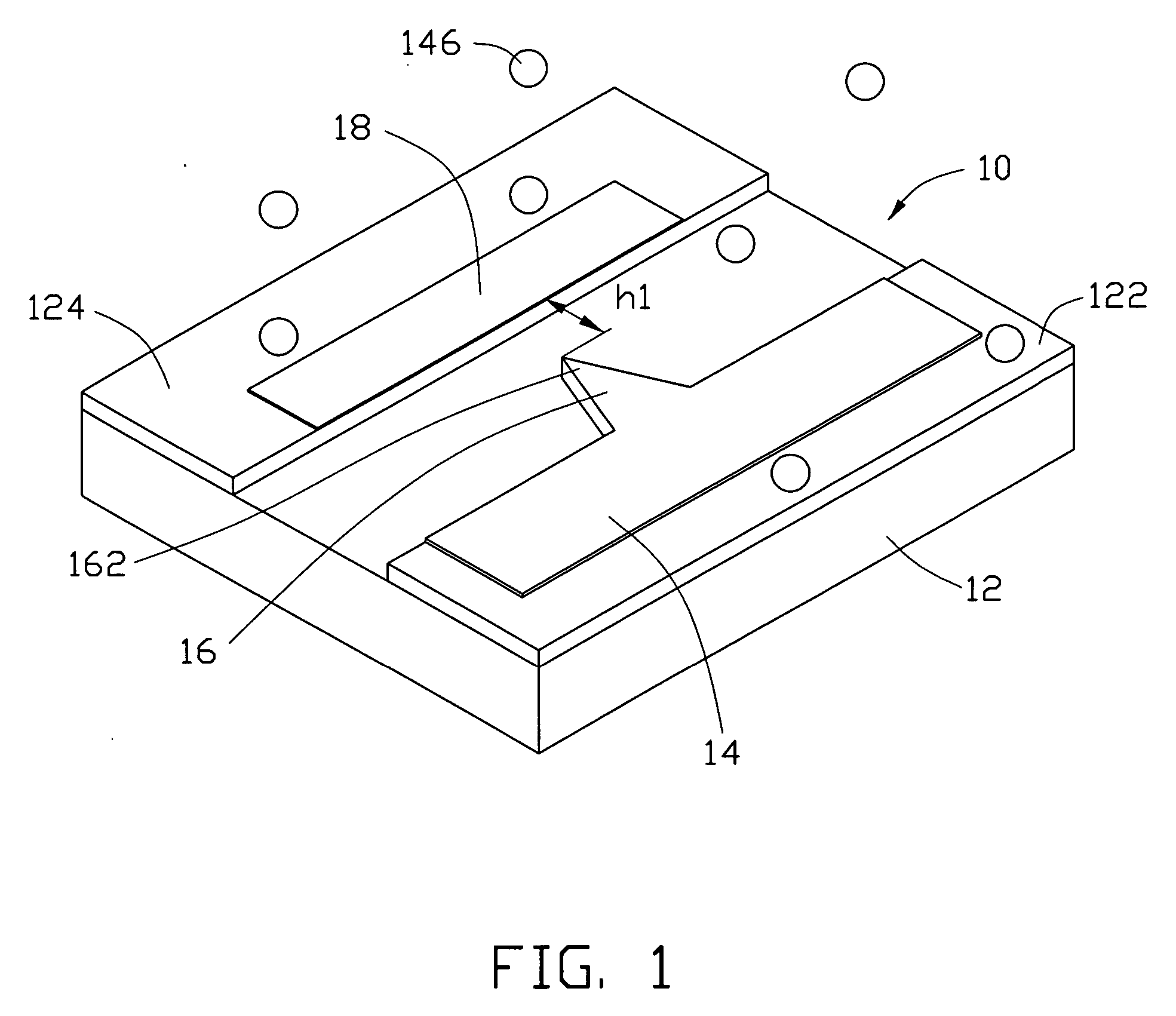
[0019]FIG. 1 shows a nano-scaled field emission electronic device 10, in accordance with the present device. As shown in FIG. 1, the nano-scaled field emission electronic device 10 is a thin-film bipolar structure and includes a substrate 12, a first insulating layer 122, a second insulating layer 124, a film of cathode electrode 14, and a film of anode electrode 18. The first insulating layer 122 and the second insulating layer 124 are respectively positioned (i.e., essentially directly deposited, which is intended to incorporate both direct attachment thereof or attachment via one or more thin, adhesion-promotion layers) on the substrate 12 and spaced from each other. The cathode electrode 14 is positioned (i.e., essentially directly deposited) on the first insulating layer 122 and has an emitter 16. The emitter 16 extends beyond the first insulating layer 122, such that a free gap exists between the emitter 16 and the substrate 12, the gap promoting free operation of the emitter ...

second embodiment

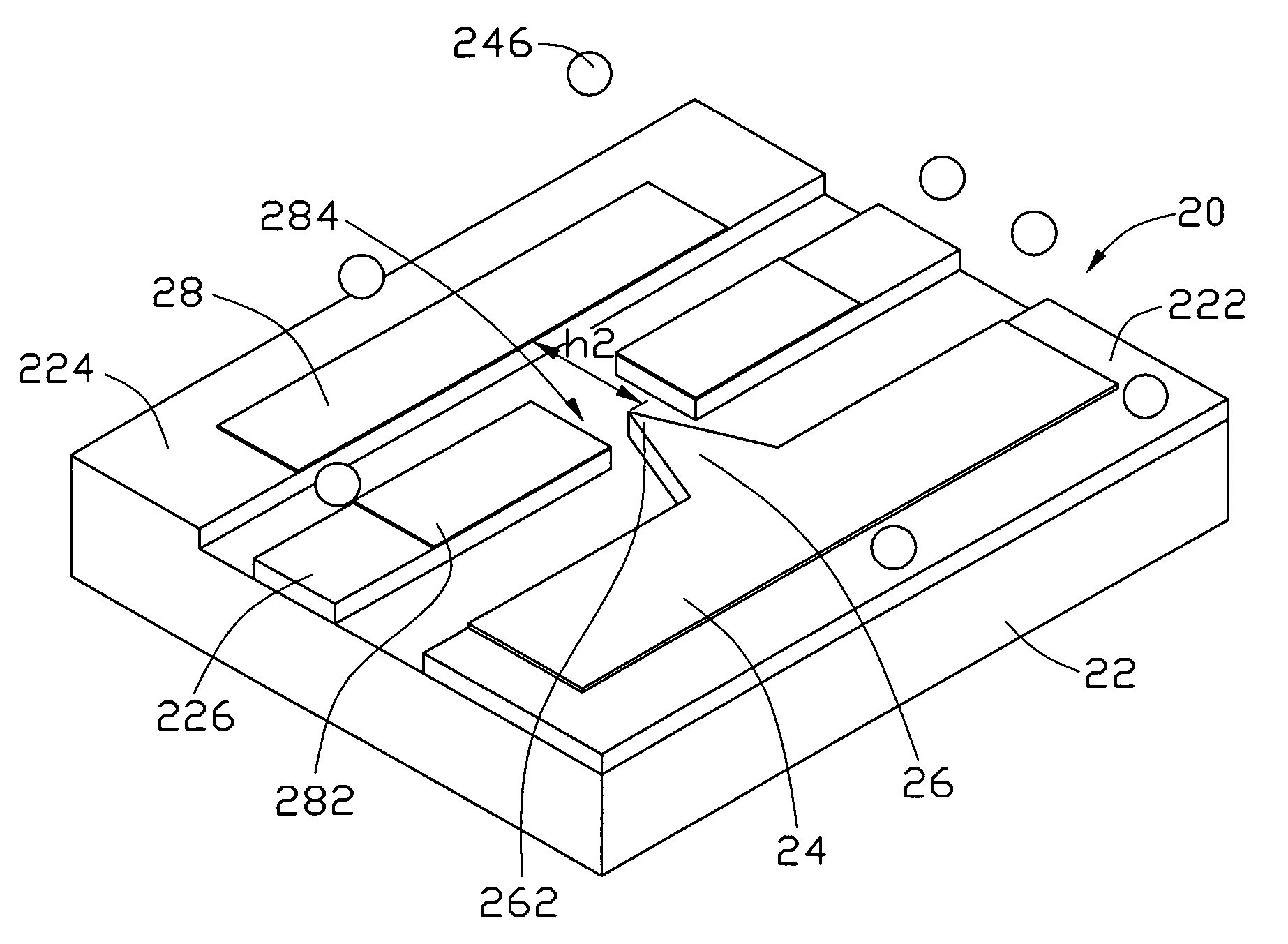
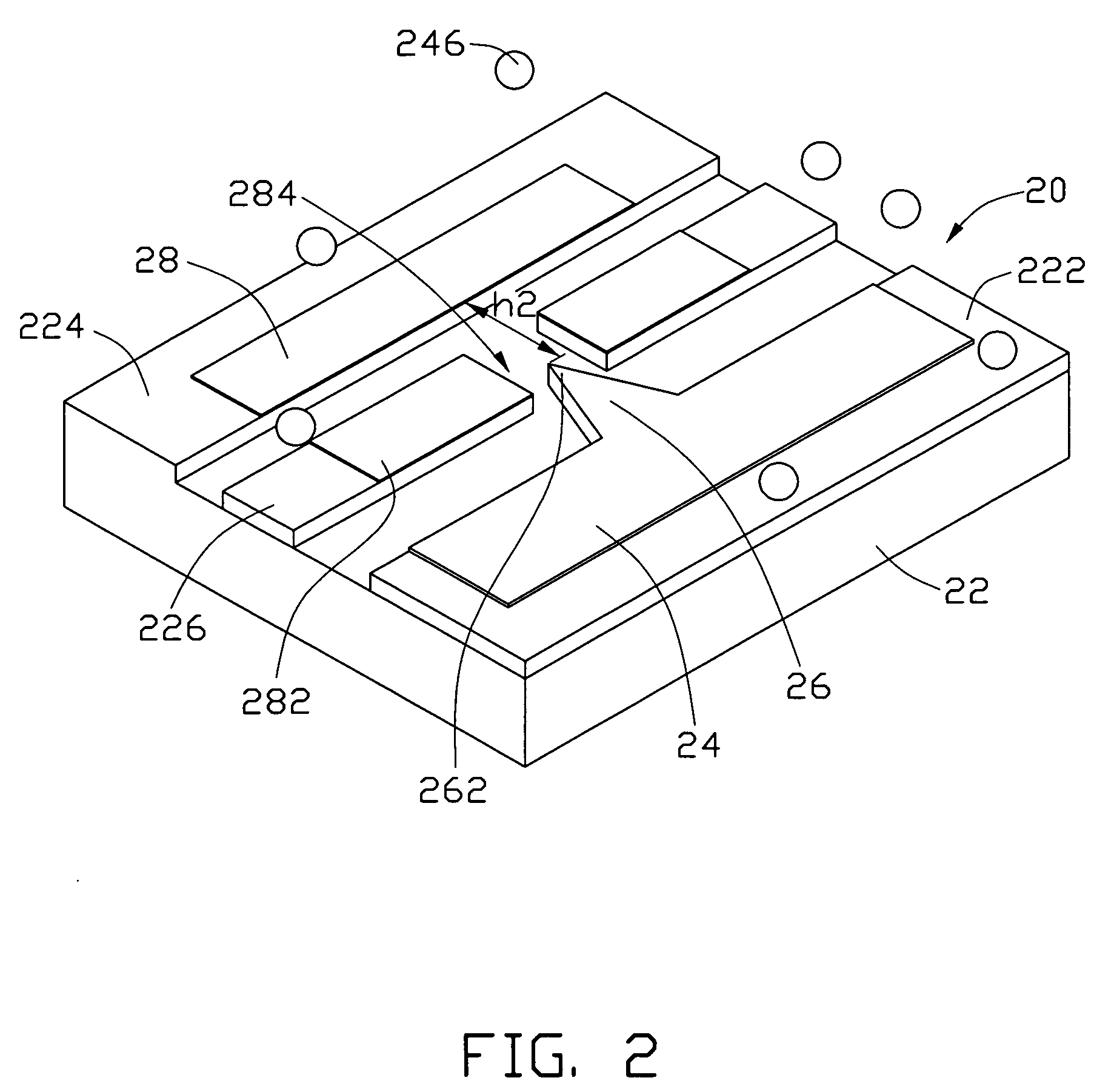
[0032] Referring to FIG. 2, a nano-scaled field emission electronic device 20 in accordance with the present device, is shown. The nano-scaled field emission electronic device 20 is a thin-film triode structure and includes a substrate 22, a first insulating layer 222, a second insulating layer 224, a third insulating layer 226, a film of cathode electrode 24, a film of grid electrode 282 and a film of anode electrode 28. The first insulating layer 222 and the second insulating layer 224 are positioned on the substrate 22 and spaced from each other. The third insulating layer 226 is positioned on the substrate 22 and spaced between the first insulating layer 222 and the second insulating layer 224. The cathode electrode 24 is positioned on the first insulating layer 222 and has an emitter 26. The emitter 26 has an emission tip 262, and the emission tip 262 faces the anode electrode 28. The anode electrode 28 is positioned on the second insulating layer 224 and apart (i.e., spaced) f...

third embodiment

[0034] Referring to FIG. 3, a nano-scaled field emission electronic device 30, in accordance with the present device, is shown. The nano-scaled field emission electronic device 30 is a thin-film triode structure and includes a substrate 22, a first insulating layer 322, a second insulating layer 324, a third insulating layer 326, a film of cathode electrode 34, a film of grid electrode 382 and a film of anode electrode 38. The first insulating layer 322 and the second insulating layer 324 are positioned on the substrate 32 and spaced from each other. The third insulating layer 326 is positioned on the substrate 32 and spaced between the first insulating layer 322 and the second insulating layer 324. The cathode electrode 34 is positioned on the first insulating layer 322 and has an emitter 36. The emitter 36 has an emission tip 362, and the emission tip 362 faces the anode electrode 38. The anode electrode 38 is positioned on the second insulating layer 324 and apart from the cathod...


PUM


Abstract

A nano-scaled field emission electronic device includes a substrate, a first insulating layer, a second insulating layer, a film of cathode electrode, and a film of anode electrode. The second insulating layer is positioned spaced from the first insulating layer. The cathode electrode is placed on the first insulating layer and has an emitter. The anode electrode is placed on the second insulating layer and positioned opposite to the cathode electrode. The nano-scaled field emission electronic device further has at least one kind of inert gas filled therein. The following condition is satisfied: h<λe, wherein h indicates a distance between a tip of the emitter and the anode electrode, and λe indicates an average free path of an electron in the inert gases. More advantageously, the following condition is satisfied: h<λe_10.

Description

RELATED APPLICATIONS [0001] This application is related to commonly-assigned application entitled, “FIELD EMISSION MICROELECTRONIC DEVICE”, filed **** (Atty. Docket No. US10587), the content of which is hereby incorporated by reference thereto. BACKGROUND [0002] 1. Field of the Invention [0003] The invention relates generally to field emission microelectronic devices and, more particularly, to a nano-scaled field emission electronic device, which is operated in an inert gases environment. [0004] 2. Discussion of Related Art [0005] The invention of computers is derived from vacuum tubes. The first computer in the world includes about 18,000 vacuum tubes. In 1947, transistors were invented by Bell laboratory. Due to the characteristic of a low energy consumption and cost, easy to be mini-sized and integrated, and suitability for mass production, transistors quickly replaced the vacuum tubes in most applied fields. This replacement made the invention of microprocessors and the mass use...

Claims


Application Information

Patent Timeline
IPC IPC(8): H01J1/02H01J1/00H01J19/06
CPCH01J21/02H01J3/021
Inventor CHEN, PI-JINHU, ZHAO-FULIU, LIANGFAN, SHOU-SHAN
Owner TSINGHUA UNIV
Why Eureka
Try Eureka