Non-volatile memory device
a memory device and non-volatile technology, applied in the field of non-volatile memory, can solve the problems of small change of a memory cell resistance value that cannot be precisely detected, the difficulty of miniaturization in lithography technique has been increased year by year, and the difficulty of retaining multi-level reliability of transistors,
- Summary
- Abstract
- Description
- Claims
- Application Information
AI Technical Summary
Problems solved by technology
Method used
Image

Examples
first embodiment
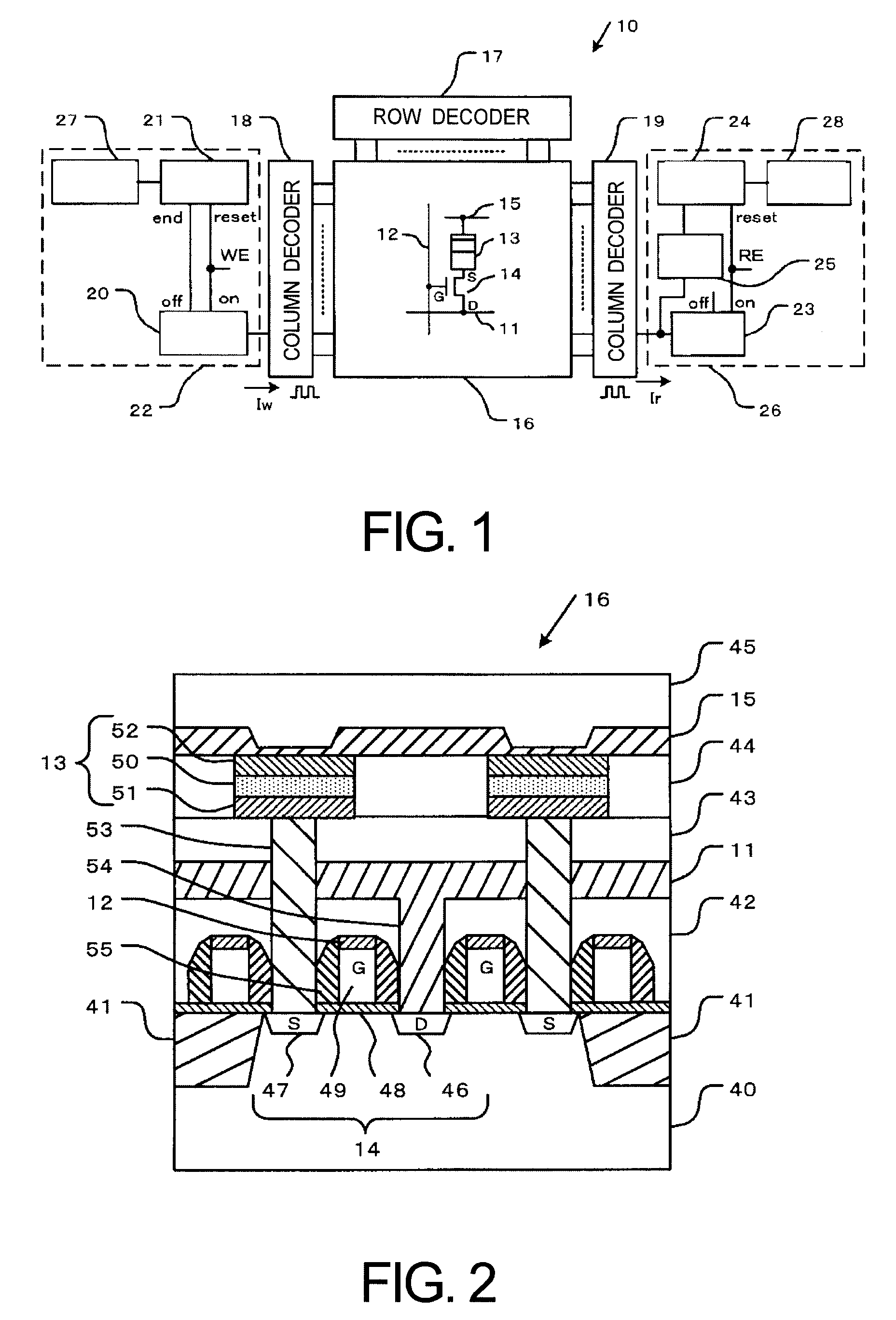
[0034] First, a non-volatile memory device according to a first embodiment of the present invention will be described below in detail with reference to FIG. 1 and FIG. 2. FIG. 1 is a block diagram showing a configuration of the non-volatile memory device. FIG. 2 is a cross-sectional view showing a structure of a memory cell array in the non-volatile memory device.
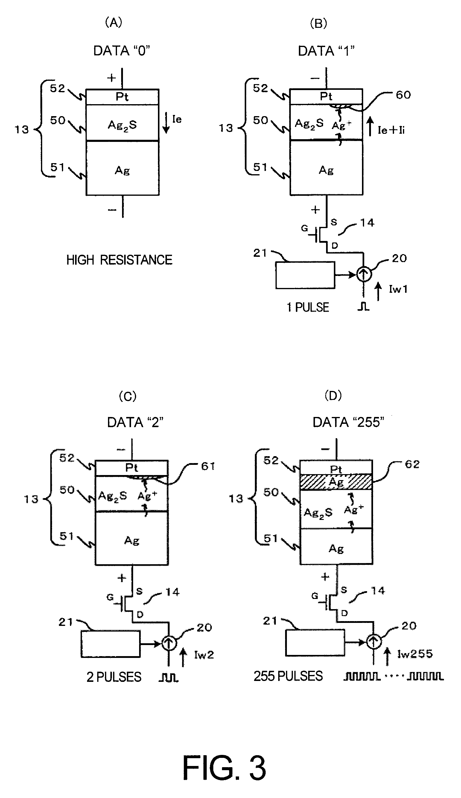
[0035] As shown in FIG. 1, the non-volatile memory device 10 according to the first embodiment provides a memory cell array 16. The memory cell array 16 provides a bit line 11, a word line 12, a memory cell 13, a cell transistor 14 and a common wiring 15. The bit line 11 and the word line 12 are arranged as a matrix. The memory cell 13 and the cell transistor 14 are disposed at an orthogonal portion between the bit line 11 and the word line 12. The memory cell 13 has an electrolyte film, a first electrode and a second electrode. The first electrode and the second electrode are formed on both surface sides of the electrolyt...
second embodiment
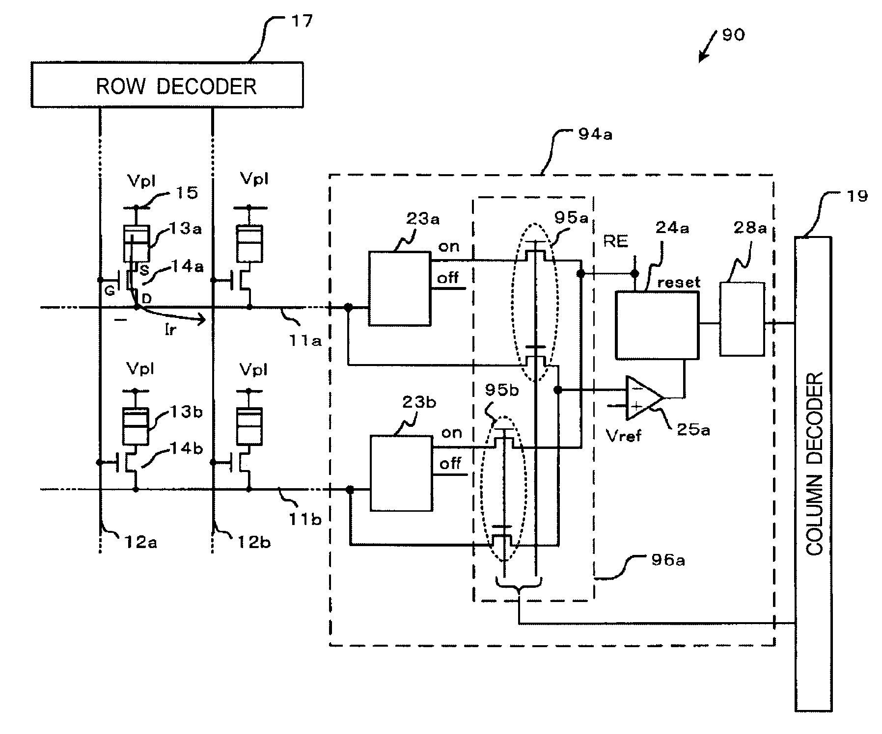
[0102]FIG. 9 is a block diagram showing a configuration of a non-volatile memory device according to a second embodiment of the present invention. In the second embodiment, a portion of a similar or same composition as the first embodiment is attached the similar or same number. Further, explanation of the portion of the similar or same composition is omitted and the portion of the different composition is explained.
[0103] A different point in the second embodiment is to configure a switching circuit which connects a data-writing means or a data-reading means to a column decoder.
[0104] As shown in FIG. 9, a non-volatile memory device 70 in this embodiment provides the switching circuit 71, for example a MOS transistor, connecting the data writing means 22 or the data-reading means 26 to the column decoder 19.
[0105] When the switching circuit 71 receives a signal WR instructing to write data into the memory cell 13, the switching circuit 71 connects the data writing means 22 to th...
third embodiment
[0109]FIG. 10 and FIG. 11 are diagrams showing a main portion of a non-volatile memory device, respectively, according to a third embodiment of the present invention. FIG. 10 is a block diagram showing a configuration of the non-volatile memory device according to the third embodiment of the present invention. FIG. 11 is a block diagram showing a configuration of a reading means of the non-volatile memory device according to the third embodiment of the present invention.
[0110] In the third embodiment, a portion of a similar or same composition as the first embodiment is attached the similar or same number. Further, explanation of the portion of the similar or same composition is omitted and the portion of the different composition is explained.
[0111] A different point in the third embodiment is to dispose the data writing means and the data-reading means on every bit line.
[0112] As shown in FIG. 9, a non-volatile memory device 80 in this embodiment is connected between the column...
PUM
 Abstract
Description
Claims
Application Information
 - R&D Engineer
- R&D Manager
- IP Professional
- Industry Leading Data Capabilities
- Powerful AI technology
- Patent DNA Extraction
Browse by: Latest US Patents, China's latest patents, Technical Efficacy Thesaurus, Application Domain, Technology Topic.
© 2024 PatSnap. All rights reserved.Legal|Privacy policy|Modern Slavery Act Transparency Statement|Sitemap