Transmission circuit and communication device

Inactive Publication Date: 2008-02-07
PANASONIC CORP
View PDF9 Cites 15 Cited by
  • Summary
  • Abstract
  • Description
  • Claims
  • Application Information

AI Technical Summary

Benefits of technology

[0016] Therefore, an object of the present invention is to provide a transmission circuit, which properly compensates for the offset characteristic of the amplitude modulat

Problems solved by technology

Accordingly, the conventional transmission circuit 600 has a problem that due to inconsistency in characteristic of these analogue components, the offset characteristic of the amplitude modulation section 504 is not properly compensated for, and distortion occurs in a transmission signal.
For this reason, the transmission circuit 600a also has a problem

Method used


Image

  • Transmission circuit and communication device
  • Transmission circuit and communication device
  • Transmission circuit and communication device

Examples


first embodiment

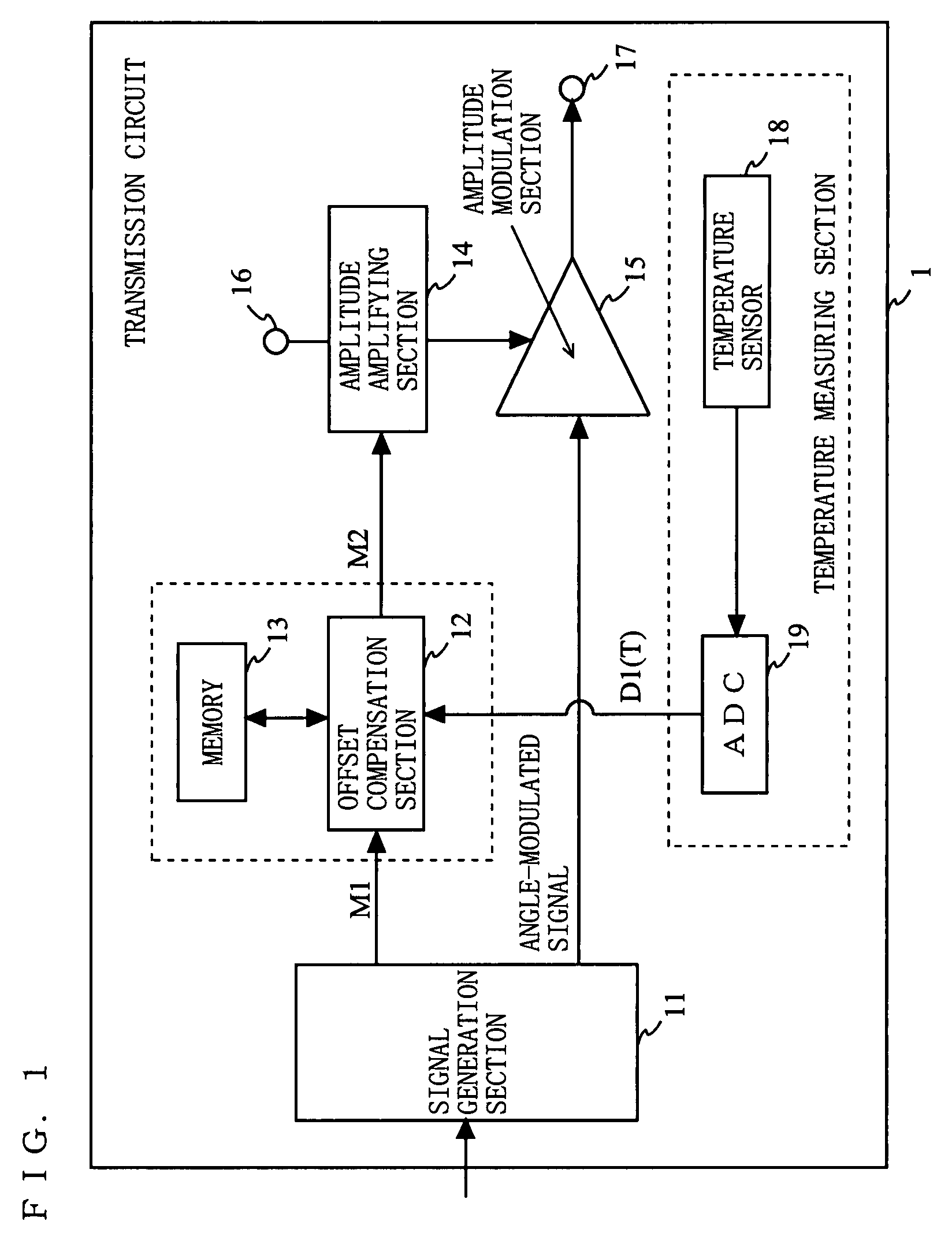
[0063]FIG. 1 is a block diagram showing an exemplary structure of a transmission circuit 1 according to a first embodiment of the present invention. In FIG. 1, the transmission circuit 1 comprises a signal generation section 11, offset compensation section 12, memory 13, amplitude amplifying section 14, amplitude modulation section 15, power supply terminal 16, output terminal 17, temperature sensor 18 and an ADC (Analogue Digital Converter) 19.

[0064] The signal generation section 11 performs predetermined signal processing on input data, thereby generating an amplitude signal M1 and an angle-modulated signal. The amplitude signal M1 is inputted to an offset compensation section 12. The offset compensation section 12 compensates for the amplitude signal M1, and outputs a resultant signal as an amplitude signal M2. The amplitude signal M2 is inputted to the amplitude amplifying section 14. The amplitude amplifying section 14 is supplied with a DC voltage from the power supply termin...

second embodiment

[0086]FIG. 8 is a block diagram showing an exemplary structure of a transmission circuit 2 according to a second embodiment of the present invention. As shown in FIG. 8, the transmission circuit 2 is different from the transmission circuit 1 of the first embodiment in that a signal generation section 11c and an amplitude amplifying section 14x have different structures from those of the signal generation section 11 and amplitude amplifying section 14. As compared to the signal generation section 11 according to the first embodiment, the signal generation section 11c further outputs power information P which is set based on a baseband. The amplitude amplifying section 14x includes the series regulator 14a and switching regulator 14b. The series regulator 14a has such a structure as shown in, e.g., FIG. 6A. The switching regulator 14b has such a structure as shown in, e.g., FIG. 6B.

[0087] Hereinafter, operations of the transmission circuit 2 will be described with reference to FIGS. ...

third embodiment

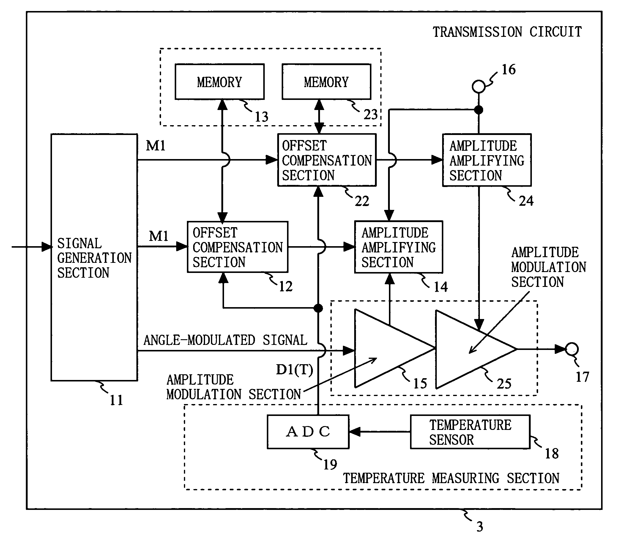
[0091]FIG. 10 is a block diagram showing an exemplary structure of a transmission circuit 3 according to a third embodiment of the present invention. As shown in FIG. 10, the transmission circuit 3 is different from the transmission circuit 1 of the first embodiment in that the amplitude modulation section is in a multiple-stage structure, and the offset characteristic of each amplitude modulation section therein is separately compensated for. It is assumed in the example shown in FIG. 3 that the transmission circuit 3 has two amplitude modulation sections (to be specific, a first amplitude modulation section 15 is provided at a previous stage to a second amplitude modulation section 25) which act as the amplitude modulation section in a multiple-stage structure.

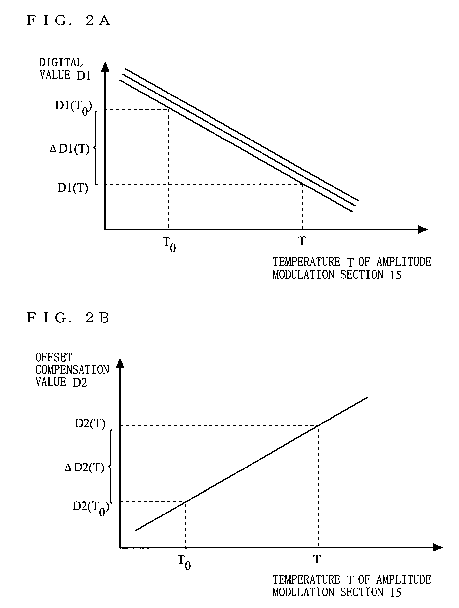
[0092]FIG. 11A shows examples of offset reference values stored in the memories 13 and 23. As shown in FIG. 11A, the digital value D1(T0), an offset compensation value D2d(T0) and a gradient αd of ΔD2d(T) with respect to ΔD...


PUM


Abstract

Provided is a transmission circuit 1 which precisely compensates for an offset characteristic of an amplitude modulation section 15 and which operates with low distortion and high efficiency over a wide output power range. A signal generation section 11 outputs an amplitude signal and an angle-modulated signal. An amplitude amplifying section 14 supplies, to the amplitude modulation section 15, a voltage corresponding to a magnitude of an inputted amplitude signal. The amplitude modulation section 15 amplitude-modulates the angle-modulated signal by the voltage supplied from the amplitude amplifying section 14, thereby outputting a resultant signal as a modulation signal. A temperature measuring section measures a temperature of the amplitude modulation section 15. An offset compensation section 12 calculates an offset compensation value in accordance with a change, in temperature of the amplitude modulation section 15, from the temperature of the amplitude modulation section 15 in an initial state, and adds the calculated offset compensation value to the amplitude signal.

Description

BACKGROUND OF THE INVENTION [0001] 1. Field of the Invention [0002] The present invention relates to a transmission circuit used for communication devices such as mobile phones and wireless LAN devices. The present invention particularly relates to a transmission circuit capable of operating with low distortion and high efficiency and a communication device using the transmission circuit. [0003] 2. Description of the Background Art [0004] Communication devices such as mobile phones and wireless LAN devices are required to, even when operating over a wide bandwidth, secure precision of a transmission signal while operating with low power consumption. For such a communication device, a transmission circuit, which is capable of outputting a transmission signal with a high precision regardless of a bandwidth and operating with high efficiency, is used. Hereinafter, conventional transmission circuits will be described. [0005] One of the conventional transmission circuits is, for example,...

Claims


Application Information

Patent Timeline
IPC IPC(8): H04K1/02
CPCH03C5/00H03F1/0205H03F1/0211H03F1/32H03F3/245H03F2200/324H04L27/361H03F2200/468H03F2200/504H04B1/0475H04B1/0483H04B2001/0425H03F2200/447H03F1/3241
Inventor MATSUURA, TORUISHIDA, KAORU
Owner PANASONIC CORP
Why Eureka
Try Eureka