Light emitting diode package

Inactive Publication Date: 2008-02-14
SAMSUNG ELECTRO MECHANICS CO LTD
View PDF2 Cites 47 Cited by
  • Summary
  • Abstract
  • Description
  • Claims
  • Application Information

AI Technical Summary

Benefits of technology

[0020] According to the present invention, the recess is formed in the bonding surface of the chip-bonded package substrate. This recess accommodates the bonding material and provides a passage for the bonding material, thereby preventing an electric short circuit due to an extra

Problems solved by technology

Such an electric short circuit among the semiconductor layers is a fatal problem, which may cause the LED chip to lose its function.
However, such a flux not only can corrode the substrate but also may increase heat resistance of the LED pac

Method used


Image

  • Light emitting diode package
  • Light emitting diode package
  • Light emitting diode package

Examples


Example

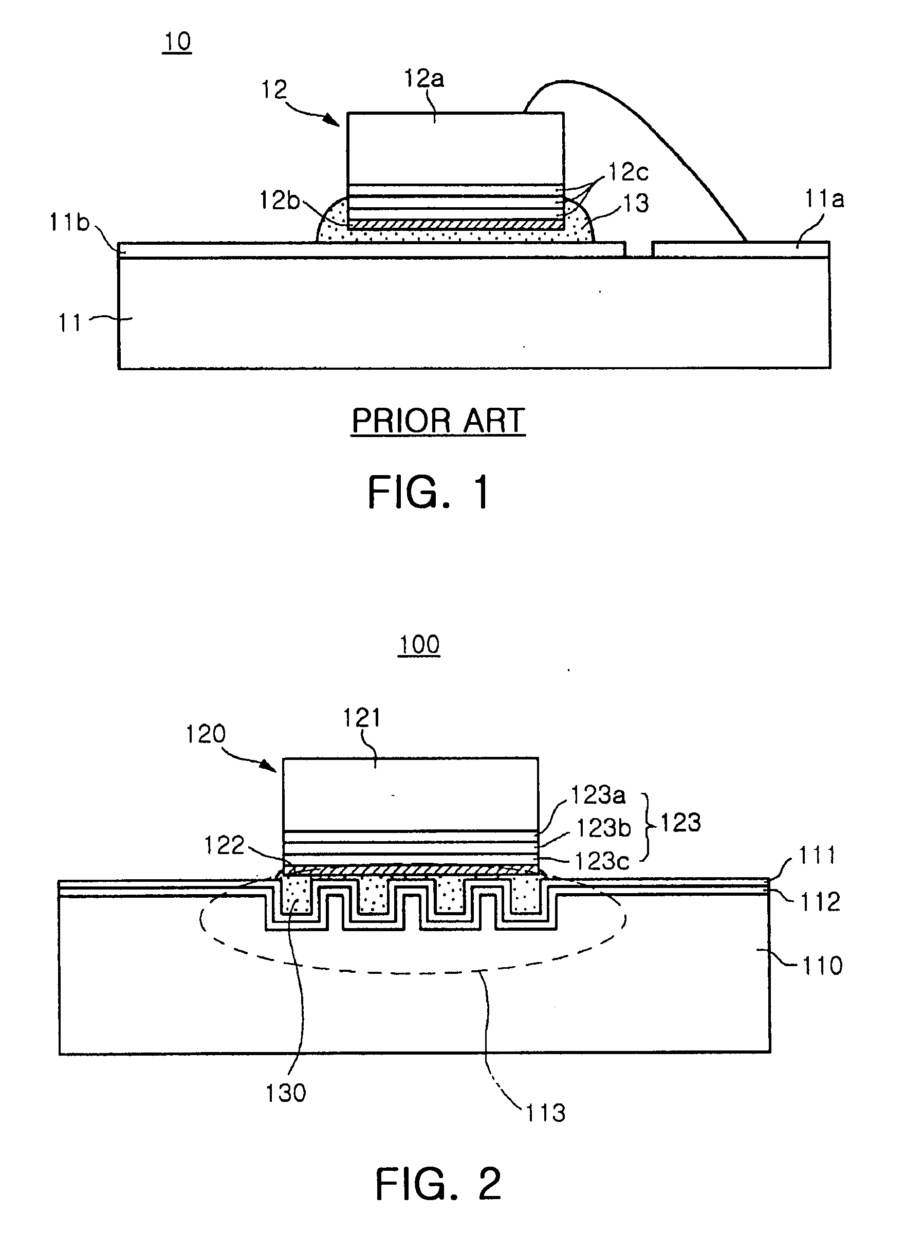
[0026] Exemplary embodiments of the present invention will now be described in detail with reference to the accompanying drawings. The invention may however be embodied in many different forms and should not be construed as limited to the embodiments set forth herein. Rather, these embodiments are provided so that this disclosure will be thorough and complete, and will fully convey the scope of the invention to those skilled in the art. In the drawings, the shapes and dimensions may be exaggerated for clarity and the same reference numerals are used throughout to designate the same or similar components.

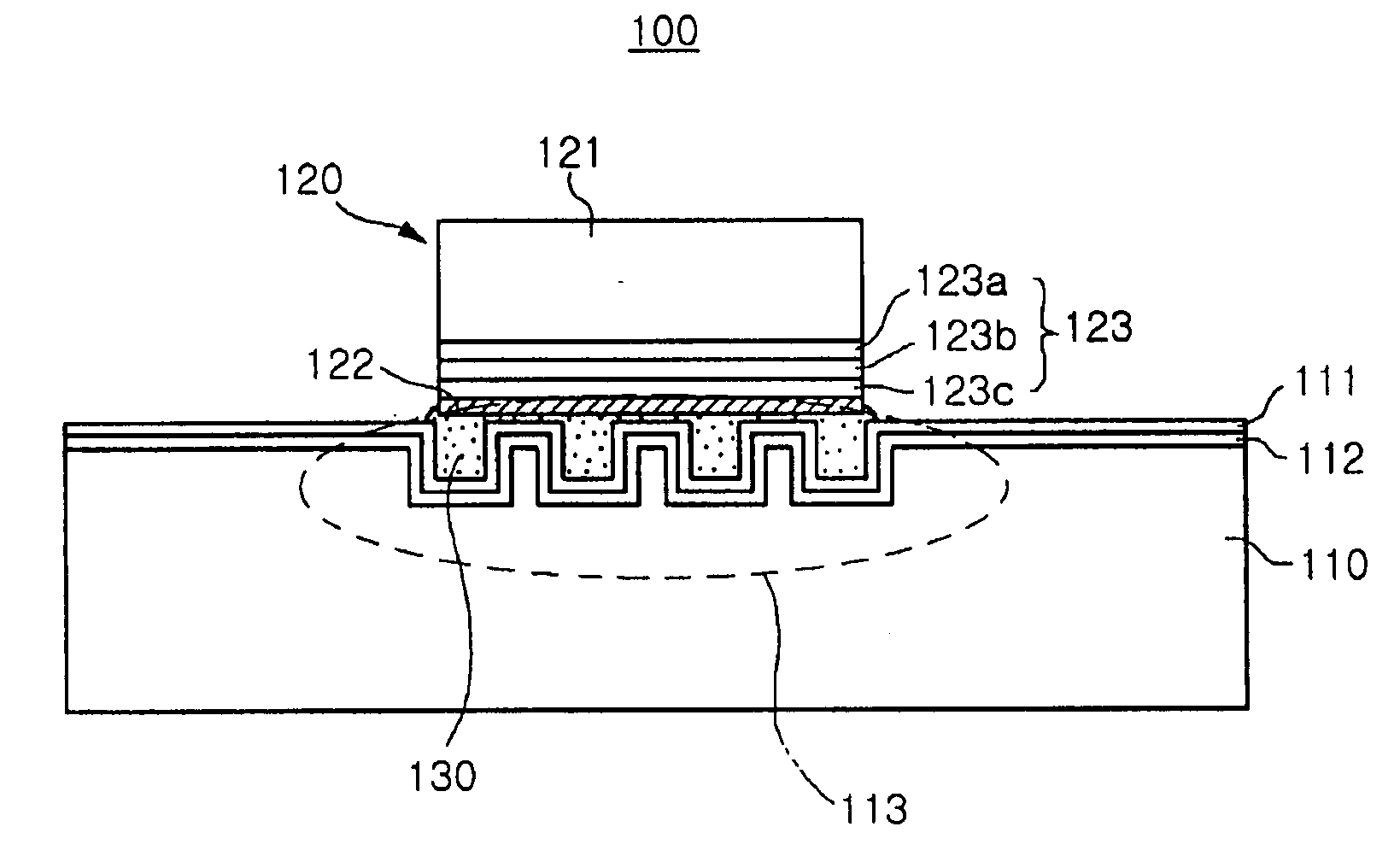
[0027]FIG. 2 is a sectional view illustrating an LED package according to an embodiment of the present invention. Referring to FIG. 2, the LED package 100 includes an LED chip 120 and a package substrate 110 on which the LED chip 120 is mounted. The LED chip 120 is a vertical-structure LED chip including a chip substrate 121 made of a conductive material such as SiC. On the chip sub...


PUM


Abstract

A light emitting diode package for preventing an electric short circuit among semiconductor layers and with excellent bonding strength. The light emitting diode package includes a package substrate, a light emitting diode chip bonded to an upper surface of the package substrate, and a bonding material for bonding the light emitting diode chip to the package substrate. The package substrate has a recess formed in a bonding surface thereof to accommodate the bonding material.

Description

CLAIM OF PRIORITY [0001] This application claims the benefit of Korean Patent Application No. 2006-0022141 filed on Mar. 9, 2006, in the Korean Intellectual Property Office, the disclosure of which is incorporated herein by reference. BACKGROUND OF THE INVENTION [0002] 1. Field of the Invention [0003] The present invention relates to a light emitting diode (hereinafter, referred to as ‘LED’) package and, more particularly, to an LED package which prevents a short circuit among semiconductor layers due to a chip bonding material and has excellent bonding strength between an LED chip and a substrate. [0004] 2. Description of the Related Art [0005] In general, a semiconductor LED has gained attention in various applications as an environmentally friendly light source that does not cause any pollution. Recently, an LED device emitting monochromatic light is combined with phosphor to provide a different wavelength of light. Such an LED product is manufactured by bonding an LED chip havin...

Claims


Application Information

Patent Timeline
IPC IPC(8): H01L33/00H01L33/40H01L33/62
CPCH01L24/29H01L24/32H01L33/62H01L2224/48091H01L2224/73265H01L2924/01013H01L2924/01029H01L2924/01032H01L2924/01033H01L2924/01047H01L2924/0105H01L2924/01078H01L2924/01079H01L2924/01082H01L2924/0132H01L2224/29H01L2224/2919H01L2224/83805H01L2924/01006H01L2924/01322H01L2924/014H01L2924/0665H01L2224/29101H01L2224/2929H01L2224/29339H01L2924/15724H01L2924/157H01L2924/15747H01L2924/15787H01L2224/83385H01L2224/29111H01L2224/32225H01L2224/48227H01L2924/00013H01L2924/12041H01L2224/26175H01L2924/00014H01L2924/00H01L2924/01014H01L2924/01028H01L2924/00012H01L2224/29099H01L2224/29199H01L2224/29299H01L24/73E05Y2800/428E06B3/2675E06B3/962E06B2003/26321
Inventor SHIN, SANG HYUNCHOI, SEOG MOONLEE, YOUNG KIKIM, YONG SIK
Owner SAMSUNG ELECTRO MECHANICS CO LTD
Why Eureka
Try Eureka