

Electro optical device and electronic apparatus
a technology of electro optical elements and electronic devices, applied in the direction of instruments, electric lighting sources, light sources, etc., can solve the problems of reducing image contrast, difficult to keep the utilization efficiency of light emitted from each electro optical element at a high level,
- Summary
- Abstract
- Description
- Claims
- Application Information
AI Technical Summary
Benefits of technology
Problems solved by technology
Method used
Image

Examples
first embodiment
A: First Embodiment
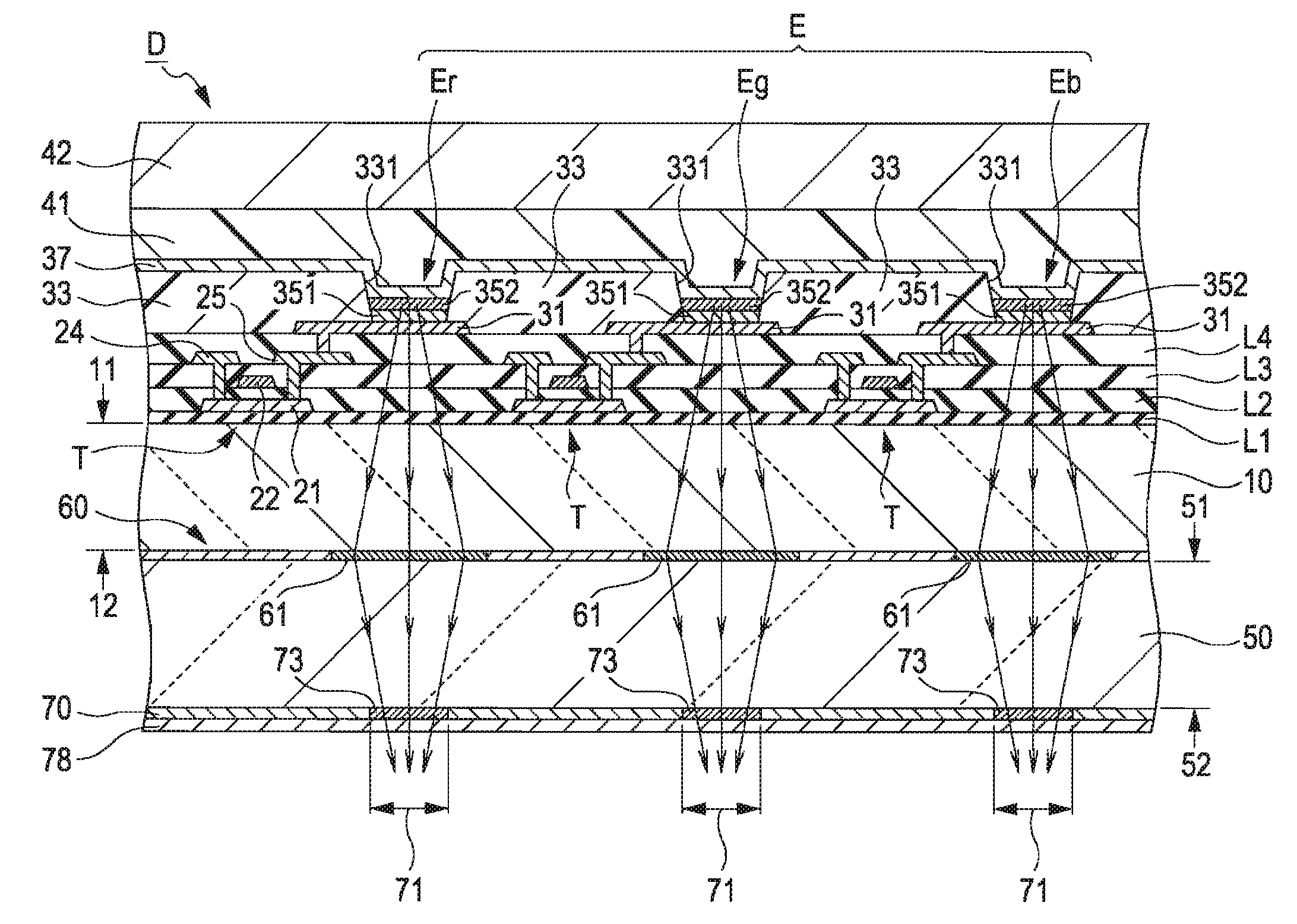
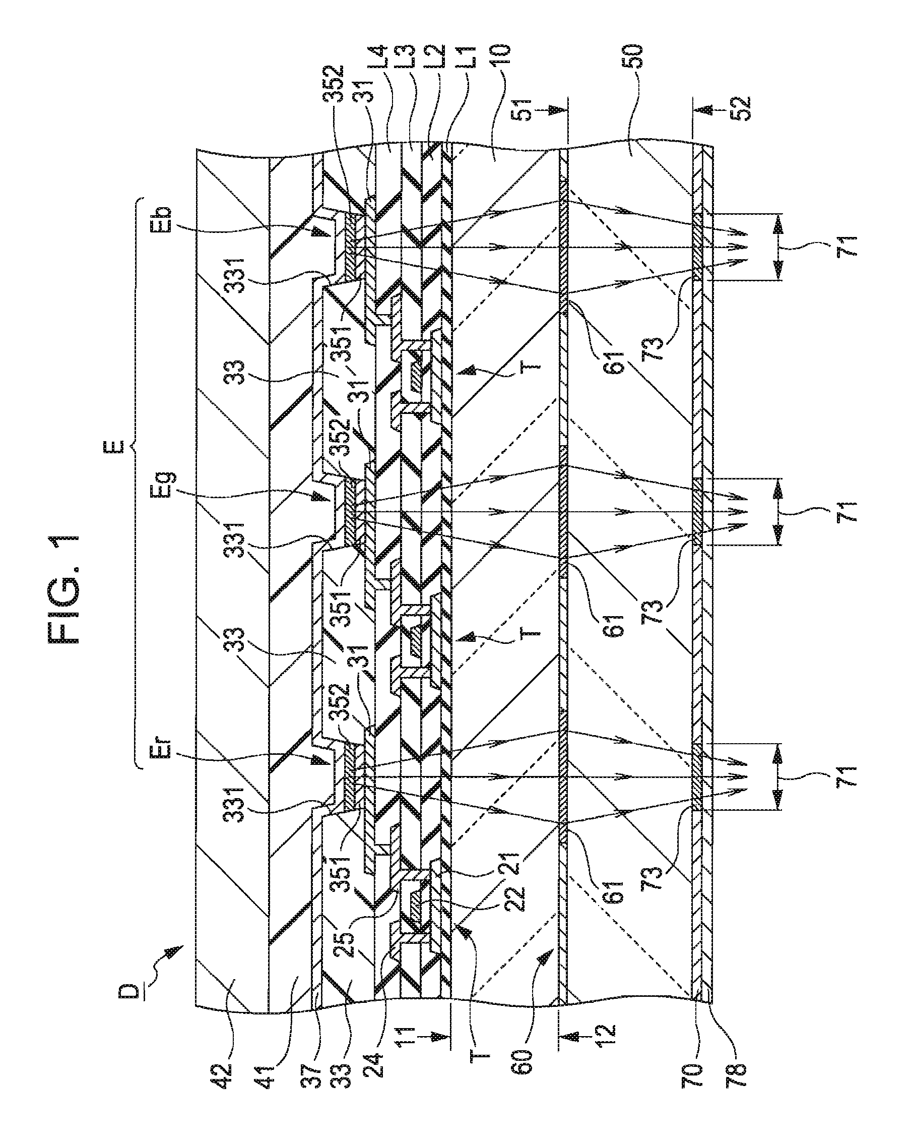
[0029]A specific embodiment of an electro optical device utilized for image display will be described with reference to FIG. 1. As shown in FIG. 1, the electro optical device D includes many electro optical elements E (Er•Eg•Eb) arranged on one surface (hereinafter, referred to as “first surface”) 11 of a substrate 10. The electro optical element E is an organic light emitting diode element (light emitting element). The electro optical elements Er is utilized for displaying red, the electro optical element Eg is utilized for displaying green, and the electro optical element Eb is utilized for displaying blue.
[0030]The substrate 10 is a flat plate having optical transparency formed by glass, plastic, or the like. The first surface 11 of the substrate 10 is covered by an insulating layer L1 over the whole region. A plurality of transistors T corresponding to the electro optical elements E are formed on the surface of the insulating layer L1. The transistor T is mean...
second embodiment
B: Second Embodiment
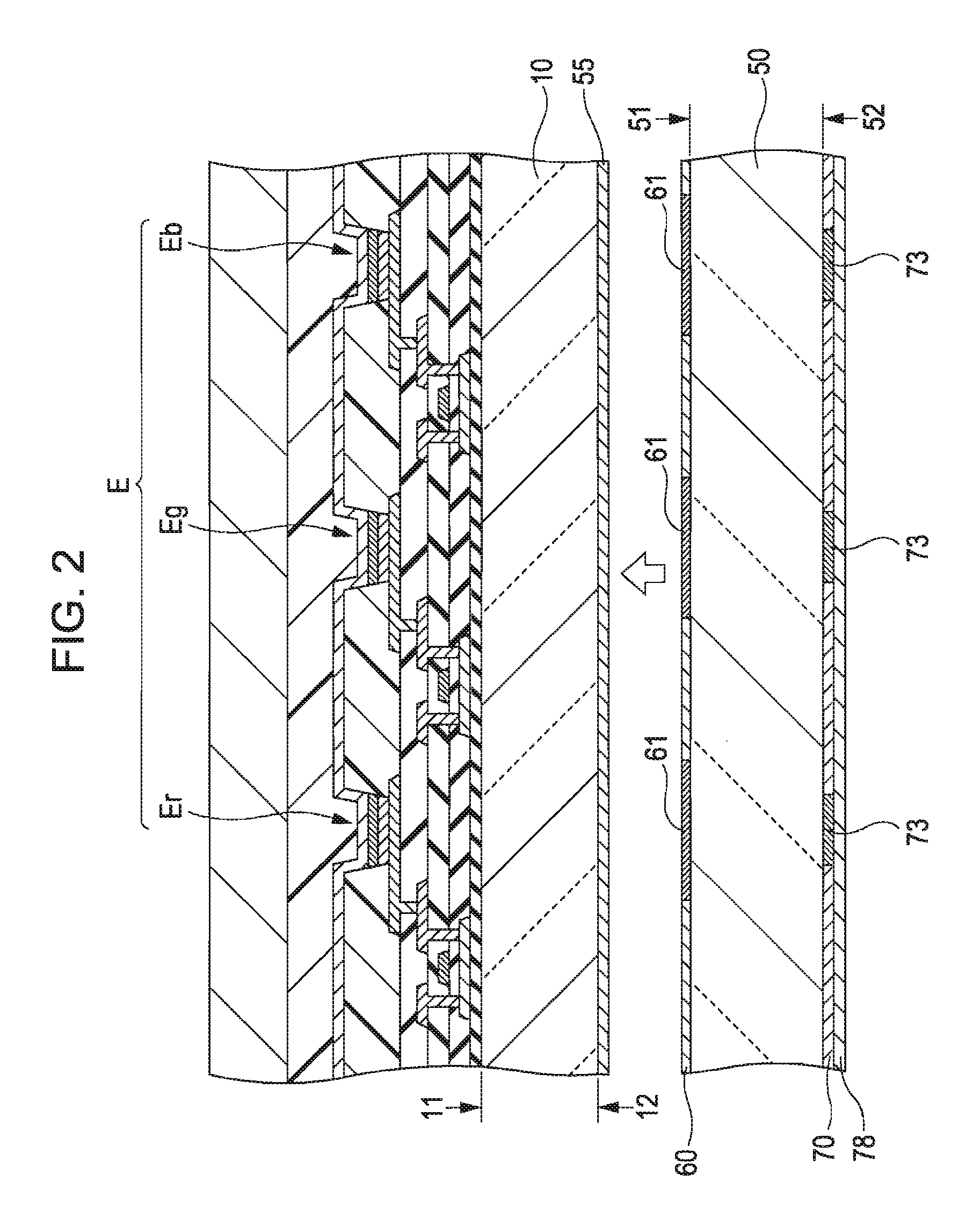
[0053]Next, a second embodiment of the invention will be described with reference to FIG. 4. Only the elements corresponding to one display color is illustrated in FIG. 4. However, the structure of the elements corresponding to the other two display colors is the same as in the first embodiment. Further, elements such as the transistors T or the like are appropriately omitted. In addition, like reference numerals are used to denote the elements having the same operation and function as the first embodiment in the embodiment, so that the detail description thereof will be appropriately omitted.
[0054]As shown in FIG. 4, in the embodiment, the hologram lens array 60 is placed on the second surface 12 of the substrate 10. The hologram lens array 60 includes many hologram lenses 61 arranged in an array manner so as to overlap each electro optical element E when viewed from the direction perpendicular to the substrate 10. Each hologram lens 61 is a reflection type posi...
modification 1
[0060]In each embodiment described above, the structure in which the emission layer 352 of each electro optical element E is formed by a separate material for each display color is exemplified. However, in the structure in which the coloring layer 73 of each display color is placed, all of the emission layers 352 of the electro optical elements E may be formed by a light emitting material which emits white light. Further, the structure in which the emission layer 352 is separated by the isolating layer 33 for each electro optical element E is not essential in the invention and the structure in which a contiguous emission layer 352 which emits white light over a plurality of elector optical elements E may be employed. With the structure, a component of the color light corresponding to a display color of the electro optical element E among the light emitted from the electro optical element E is selectively emitted from the coloring layer 73. For the formation of the contiguous emissio...
PUM
 Abstract
Description
Claims
Application Information