Electronic Device Test Apparatus and Method of Configuring Electronic Device Test Apparatus

a technology of electronic devices and test apparatuses, which is applied in the direction of measurement devices, semiconductor/solid-state device testing/measurement, instruments, etc., can solve the problems of increasing equipment costs, not being efficient, and not necessarily achieving maximum throughput, etc., and achieve the effect of efficiency of test apparatus

a technology of electronic devices and test apparatuses, which is applied in the direction of measurement devices, semiconductor/solid-state device testing/measurement, instruments, etc., can solve the problems of increasing equipment costs, not being efficient, and not necessarily achieving maximum throughput, etc., and achieve the effect of efficiency of test apparatus

US20080042667A1Inactive Publication Date: 2008-02-21ADVANTEST CORP

Image

  • Electronic Device Test Apparatus and Method of Configuring Electronic Device Test Apparatus
  • Electronic Device Test Apparatus and Method of Configuring Electronic Device Test Apparatus
  • Electronic Device Test Apparatus and Method of Configuring Electronic Device Test Apparatus

Examples


first embodiment

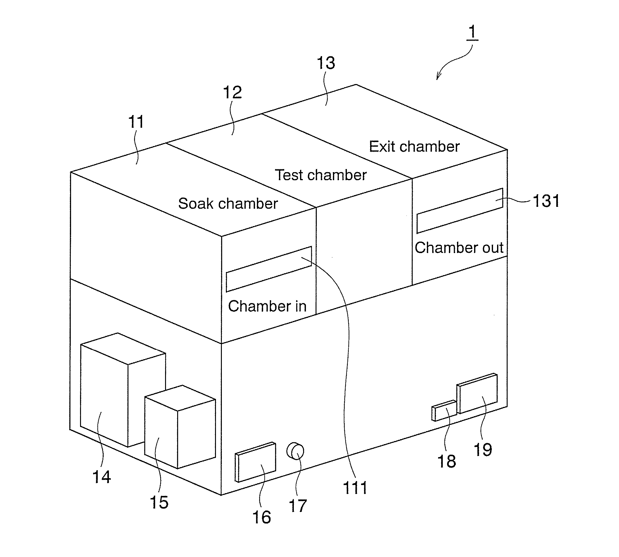
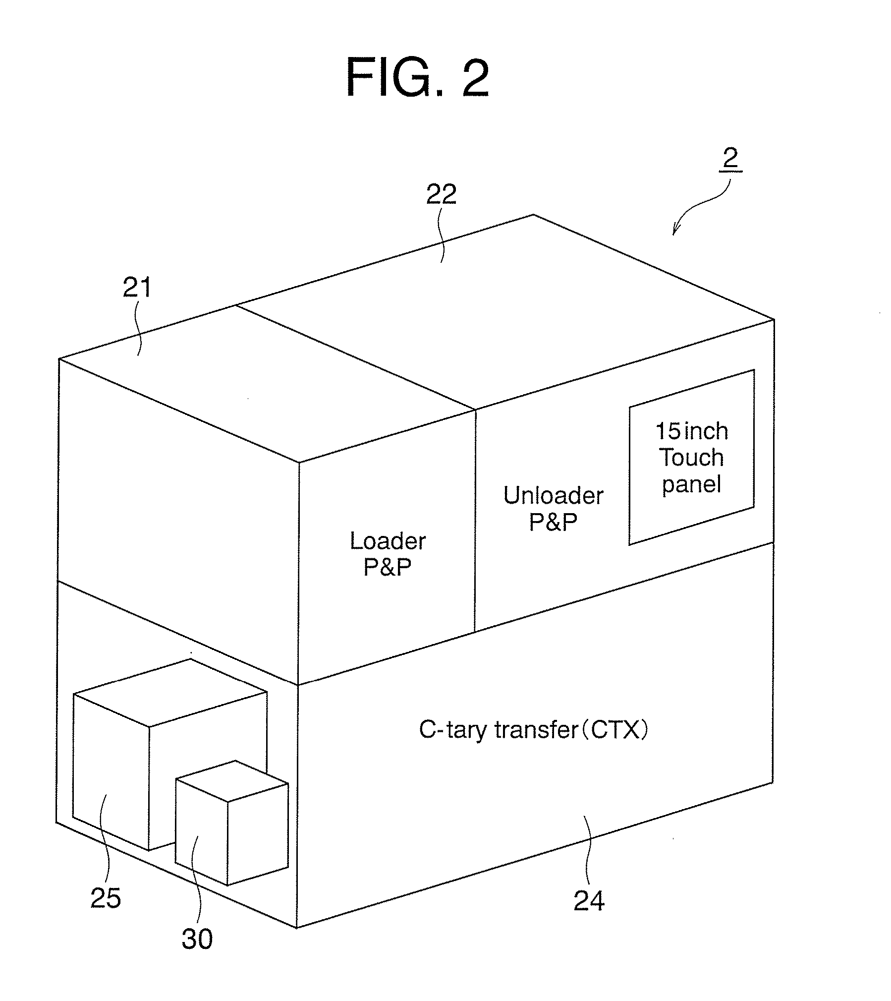
[0085]FIG. 1 is a schematic view of a first embodiment of a test module according to the present invention, FIG. 2 is a schematic view (front view) of the first embodiment of a handling module according to the present invention, FIG. 3 is a schematic view of the same (back view), FIG. 4 is a view for explaining the combination of the types of the handling modules and test modules according to the present invention, FIG. 5 is a conceptual view of the method of transporting DUTs and trays in the electronic device test apparatus according to the present invention, FIG. 6 is a view for explaining a selection method based on the number of simultaneous measurements of the test module according to the present invention, and FIG. 7 is a view for explaining a selection method based on the throughput of the handling module and the number of simultaneous measurements of the test module according to the present invention. Note that FIG. 5 is a view for explaining the method of transporting DUTs...

second embodiment

[0114]FIG. 8 is a disassembled perspective view of a second embodiment of a handler according to the present invention, while FIG. 9 is a perspective view of the handler shown in FIG. 8 assembled.

[0115] The handler according to the present embodiment is comprised of a contact module 3, eject module 4, loader module 5, unloader module 6, and stocker module 7. These modules 3 to 7 comprise the lower level units 11 to 13, 21, 22, and 24 of the test module 1 and handling module 2 in the first embodiment formed into modules. There, this ā€œmodularizationā€ means forming the units forming the electronic device test apparatus to be separable and connectable from and to their adjoining units and preparing two or more units of different specifications as replacement units.

[0116]FIG. 10 is a side view of a pusher module in the second embodiment of the present invention, FIG. 11A and FIG. 11B are plan views showing variations of a pusher module, FIG. 12 is a side view of a contact arm module, a...


PUM


Abstract

A handler is configured by, separably and connectably, a plurality of types of handling modules of different throughputs and a plurality of types of test modules of different numbers of simultaneous measurements and / or test temperatures. Based on the maximum number of measurable pins of the tester outputting a test pattern and examining a response pattern, the number of terminals of the DUTs, and the test time, the throughput of the handling module and the number of simultaneous measurements and / or test temperature of the test module are selected and combined.

Description

BACKGROUND OF THE INVENTION [0001] 1. Field of the Invention [0002] The present invention relates to an electronic device test apparatus for testing semiconductor integrated circuit devices and various other electronic devices and a method of configuring an electronic device test apparatus, more particularly relates to an electronic device test apparatus enabling optimization so that the efficiency of the test apparatus as a whole does not fall due to the performance of a handler even when maximum number of simultaneous measurements has been changed due to the relationship between the maximum number of testable pins of the tester and the number of pins of an electronic device under test (DUT) and a method of configuring such an electronic device test apparatus. [0003] 2. Description of the Related Art [0004] In the process of production of semiconductor devices, an electronic device test apparatus becomes necessary for testing the finally produced IC chip or other electronic device....

Claims


Application Information

Patent Timeline
21 Feb 2008
Publication
US20080042667A1
IPC
G01R31/28
CPC
G01R31/2868; G01R31/2893; G01R31/2865; G01R31/31905; G01R31/31718; G01R31/26; H01L22/00
Inventors
YAMASHITA, KAZUYUKI; MASUO, YOSHIYUKI