Laminating System

Inactive Publication Date: 2008-02-21
SEMICON ENERGY LAB CO LTD
View PDF18 Cites 116 Cited by
  • Summary
  • Abstract
  • Description
  • Claims
  • Application Information

AI Technical Summary

Benefits of technology

[0018] In a laminating system according to the present invention in which a roller for supplying a substrate for sealing, a roller for winding thin film integrated circuits, rollers for separating and sealing the thin film integrated circuits, the separation, sealing, and reception of the plurality of thin film integrated circuits provided over a substrate can be carried out continuously; thus, the production efficiency can be improved and the manufacturing time can be reduced.
[0019] Further, a laminating system according to the

Problems solved by technology

Further, as described above, a thin film integrated circuit is broken very easily, and attention is required to

Method used


Image

  • Laminating System
  • Laminating System
  • Laminating System

Examples


embodiment mode 1

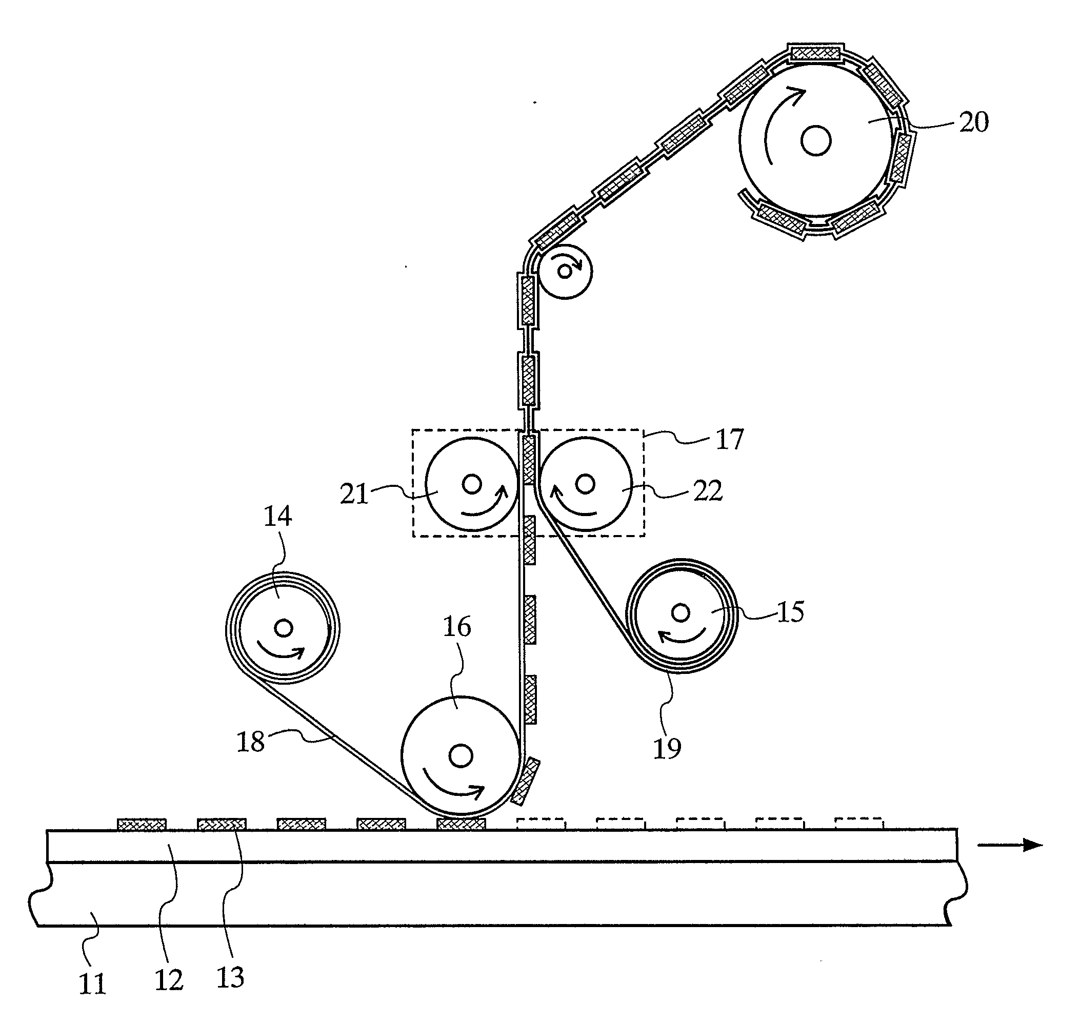
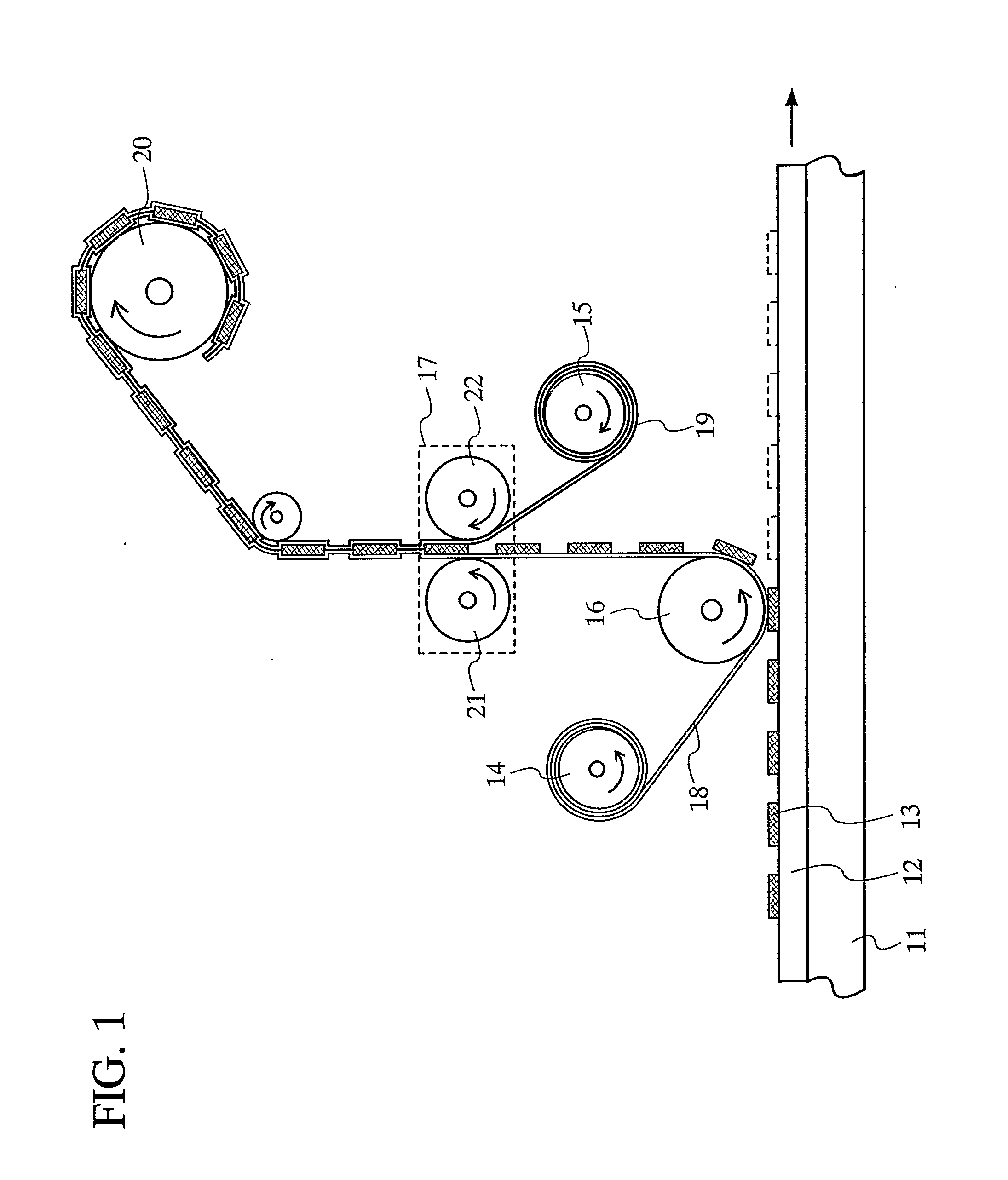
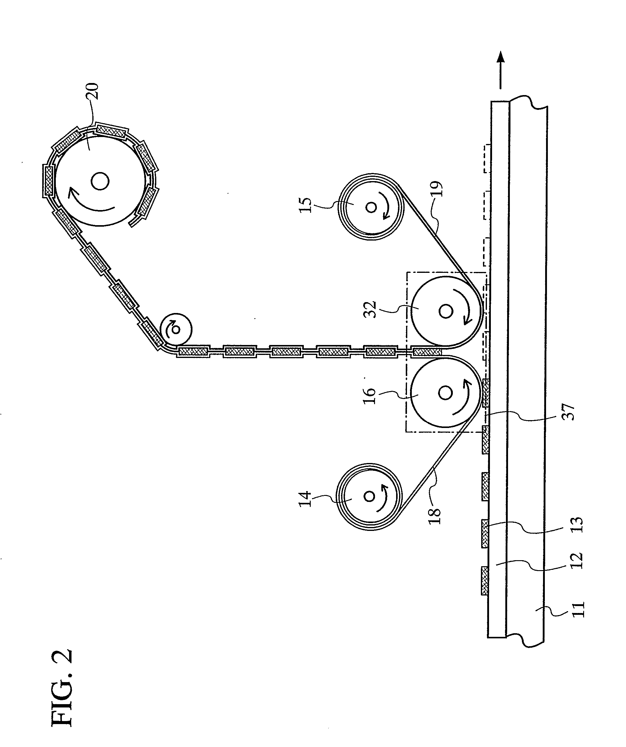
[0035] The invention provides a laminating system in which rollers are used for supplying a substrate for sealing, receiving IC chips, separating, and sealing. Major modes of the laminating system will be described with reference to the drawings.

[0036] A laminating system according to the invention comprises: a transfer means 11 for transferring a first substrate 12 provided with a plurality of thin film integrated circuits 13, a first supplying roller 14 on which a second substrate 18 winds, a peeling roller 16 which separates the thin film integrated circuits 13 from the first substrate 12, a second supplying roller 15 on which a third substrate 19 winds, a laminating means 17 which seals the thin film integrated circuits 13 between the second substrate 18 and the third substrate 19, and a receiving roller 20 on which the sealed thin film integrated circuits 13 wind (FIG. 1).

[0037] In an apparatus shown in FIG. 1, thin film integrated circuits 13 over the first substrate 12 whic...

embodiment mode 2

[0073] A structure of an IC sheet (also referred to as an IC film, a sheet element, and a film element) according to the invention will be described. An IC sheet according to the invention is a second substrate 18 and a third substrate 19 which are attached to each of a plurality of thin film integrated circuits 13 from both surfaces which are wound in a roller shape (see cross-sectional view of an IC sheet in FIG. 13). Each of the plurality of thin film integrated circuits 13 has a plurality of elements and a conductive layer serving as an antenna. Each of the plurality of thin film integrated circuits 13 are arranged regularly.

[0074] As described above, sheet-like IC sheets comprising a plurality of thin film integrated circuits 13 sealed with a pair of substrates for sealing are easy to be shipped. In particular, it is advantageous in the shipment of a large amount of thin film integrated circuits 13. Further, the plurality of thin film integrated circuits 13 are difficult to be...

embodiment mode 3

[0075] A structure of a roll (also referred to as wound element, roll body or the like) according to the invention will be described. A roll according to the invention winds a substrate, more specifically, a second substrate 18 and a third substrate 19 which seal each of a plurality of thin film integrated circuits 13 are wound in a roll shape (see a cross-sectional view of a roll in FIG. 12A and a perspective view of a roll in FIG. 12B). Each of the plurality of thin film integrated circuits 13 has a plurality of elements and a conductive film as an antenna. The plurality of thin film integrated circuits 13 are arranged regularly.

[0076] As described above, a roll which is a plurality of thin film integrated circuits 13 sealed with a pair of substrates are wound can easily be shipped. In particular, it is advantageous in the shipment of a large amount of thin film integrated circuits 13. Further, the plurality of thin film integrated circuits 13 are difficult to be handled when eac...


PUM

PropertyMeasurementUnit
Pressureaaaaaaaaaa
Adhesivityaaaaaaaaaa

Abstract

It is an object of the invention to improve the production efficiency in sealing a thin film integrated circuit and to prevent the damage and break. Further, it is another object of the invention to prevent a thin film integrated circuit from being damaged in shipment and to make it easier to handle the thin film integrated circuit. The invention provides a laminating system in which rollers are used for supplying a substrate for sealing, receiving IC chips, separating, and sealing. The separation, sealing, and reception of a plurality of thin film integrated circuits can be carried out continuously by rotating the rollers; thus, the production efficiency can be extremely improved. Further, the thin film integrated circuits can be easily sealed since a pair of rollers opposite to each other is used.

Description

TECHNICAL FIELD [0001] The present invention relates to a laminating system which seals a thin film integrated circuit. The invention further relates to an IC sheet including a plurality of thin film integrated circuits which are sealed. The invention still further relates to a roll of a plurality of thin film integrated circuits which are sealed and wound. Moreover, the invention relates to a method for manufacturing an IC chip in which a thin film integrated circuit is sealed. BACKGROUND ART [0002] In recent years, a technology of an IC chip using a thin film integrated circuit provided over a glass substrate (also referred to as IC tag, ID tag, RF (Radio Frequency) tag, wireless tag, or electronic tag) has been developed. In such technology, a thin film integrated circuit provided over a glass substrate is required to be separated from the glass substrate, which is a supporting substrate, after the completion. Accordingly, as a technology for separating a thin film integrated cir...

Claims


Application Information

Patent Timeline
IPC IPC(8): H01L21/67B42D15/10G06K19/07G06K19/077H01L21/00H01L21/336H01L21/56H01L21/68H01L21/77H01L21/84H01L27/12H01L29/786
CPCB32B37/20Y10T156/1089B42D2033/46G06K19/07718G06K19/07749G06K19/0775H01L21/67126H01L21/67132H01L21/67144H01L21/6835H01L27/1214H01L27/1266H01L2221/68318H01L2221/68354H01L2221/68363H01L2924/19041H01L21/56H01L2924/0002B32B2305/342Y10T156/1712Y10T156/1093H01L2924/00H01L23/28B42D25/45
Inventor WATANABE, RYOSUKETAKAHASHI, HIDEKAZUTSURUME, TAKUYA
Owner SEMICON ENERGY LAB CO LTD
Why Eureka
Try Eureka