Stackable packages for three-dimensional packaging of semiconductor dice

a technology of stackable packages and semiconductor dice, which is applied in the direction of semiconductor devices, semiconductor/solid-state device details, electrical equipment, etc., can solve the problems of prone to bending, increased package footprint, and expensive trimming tools

Active Publication Date: 2008-02-28
ATMEL CORP
View PDF28 Cites 101 Cited by
  • Summary
  • Abstract
  • Description
  • Claims
  • Application Information

AI Technical Summary

Benefits of technology

[0012]An inner portion is located between and electrically isolated from the pair of outer portions. The inner portion is thinner than the sidewall area of the parallel outer portions and is designed to serve as an attachment area for an integrated circuit die or other electrical component. A combined thickness of the inner portion and the integrated circuit die (or component) is less than a height of the sidewall area. This mounting arrangement leaves an uppermost portion of the sidewall areas electrically exposed for mounting additional leadless packages or other components on top of the first package.
[0013]In another exemplary embodiment, the present invention is a method of packaging a semiconductor device. The method includes mounting an electrical component to an inner portion die pad where the die pad is a portion of a substrate strip component of a first leadless three-dimensional stackable semiconductor package. A plurality of bond wires is secured from a plurality of bond pads on the electrical component to corresponding ones of a plurality of wirebond pads contained on a leadless outer portion of the substrate strip component. The outer portion has a sidewall that has a height greater than a combined height of the electrical component and the inner portion die pad.

Problems solved by technology

When a conventional plastic package having leads along the perimeter of the package must accommodate a large number of electrical connection points, the footprint of the package increases.
However, a pin pitch of less that about 0.4 mm gives rise to many technical concerns.
For example, trimming of a package having a pin pitch less than 0.4 mm requires expensive trimming tools, and the leads are prone to bending during handling of the package.
In addition, surface-mounting of such packages demands a costly and complicated surface-mounting process due to a required critical alignment step.
Accordingly, chip scale packages use specialized packaging materials and processes that increase package manufacturing costs.

Method used


Image

  • Stackable packages for three-dimensional packaging of semiconductor dice
  • Stackable packages for three-dimensional packaging of semiconductor dice
  • Stackable packages for three-dimensional packaging of semiconductor dice

Examples


Embodiment Construction

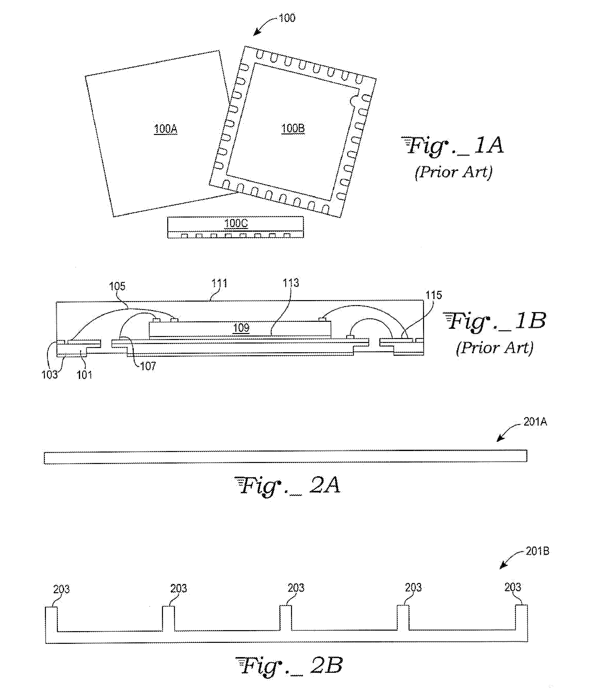
[0021]In FIG. 2A, a substrate strip 201A is selected to have a thickness close to a final “height” of a completed package. The height chosen for the substrate strip 201A will be based on particular components placed in the final package but will typically vary from 0.2 mm to 2 mm. Additional details to determine an actual height for a given package will be discussed in greater detail, infra.

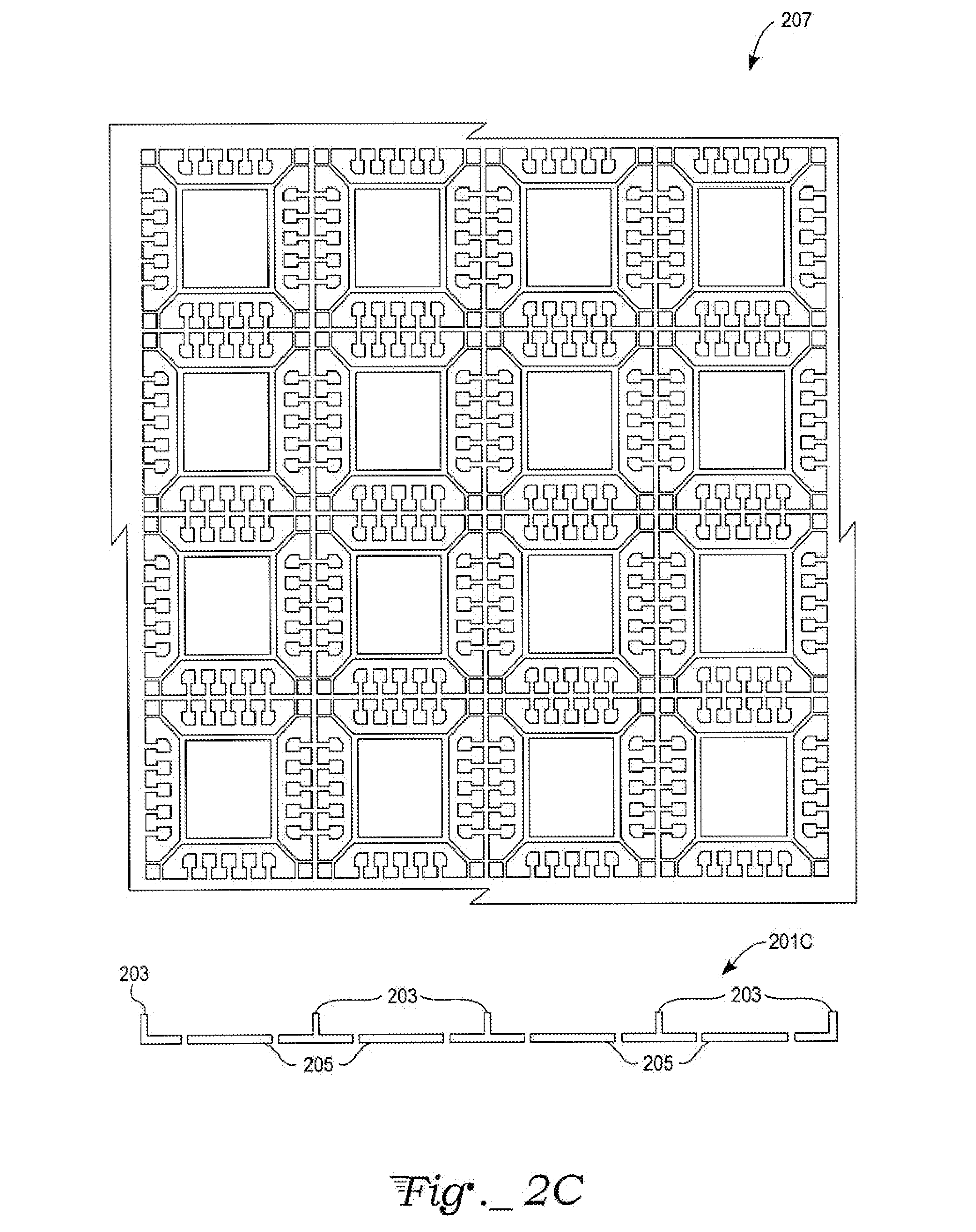
[0022]Processes described herein refer to exemplary embodiments where many packages are formed in an X-Y matrix, although a single package could readily be formed by the same process as well. The X-Y matrix size for the substrate strip 201A may be chosen to suit a particular vendor's tooling. In a specific exemplary embodiment, the X-Y dimensions of the substrate may be 205 mm×60 mm and the construction material is selected to be copper. In other exemplary embodiments, the substrate 201A may be another type of metallic or non-metallic material. The material may be either electrically conductive o...


PUM


Abstract

An apparatus and a method for packaging semiconductor devices. The apparatus includes a substrate strip component of a leadless three-dimensional stackable semiconductor package having mounting contacts on, for example, four peripheral edges. The substrate strip may either be fabricated for mounting a single electrical component (e.g., an integrated circuit die) or a plurality of substrate strips may be laid out in an X-Y matrix pattern which may later be singulated into individual package strip for leadless packages. Three-dimensional stacking is achieved by a bonding area on an uppermost portion of the sidewall. The sidewall of the strip is high enough to enclose an encapsulant covering a later mounted integrated circuit die and associated bonding wires.

Description

TECHNICAL FIELD[0001]The invention relates to a three-dimensional stackable semiconductor package, and more particularly, to a three-dimensional stackable semiconductor package for package types involving no-lead packages.BACKGROUND ART[0002]As semiconductor integrated circuit chips become more multi-functional and highly integrated, the chips include more bonding pads (or terminal pads), and thus packages for the chips have more external terminals (or leads). When a conventional plastic package having leads along the perimeter of the package must accommodate a large number of electrical connection points, the footprint of the package increases. However, a goal in many electronic systems is to minimize an overall size of the systems. Thus, to accommodate a large number of pins without increasing the footprint of package, pin pitch (or lead pitch) of the package must decrease. However, a pin pitch of less that about 0.4 mm gives rise to many technical concerns. For example, trimming ...

Claims


Application Information

Patent Timeline
Patent Type & Authority Applications(United States)
IPC IPC(8): H01L23/02
CPCH01L21/561H01L24/45H01L2924/15747H01L2225/1058H01L25/03H01L2924/01028H01L2924/12041H01L2225/1029H01L2924/014H01L2924/01033H01L2924/01006H01L2224/73265H01L2224/32245H01L2224/32257H01L2924/19107H01L2924/14H01L2924/01082H01L2924/01079H01L2924/01078H01L2924/0105H01L2924/01047H01L2924/01046H01L2924/01029H01L2924/01015H01L2924/01013H01L2224/97H01L2224/48257H01L2224/48247H01L24/97H01L25/105H01L2224/45124H01L2224/45144H01L2224/48091H01L2924/00014H01L2224/85H01L2924/00H01L2924/00012H01L24/73H01L2924/181
Inventor LAM, KEN M.
Owner ATMEL CORP
Why Eureka
Try Eureka