Method and apparatus for silicon-on-insulator material characterization

a technology of silicon-on-insulator material and characterization method, which is applied in the direction of photometry using electric radiation detector, semiconductor/solid-state device testing/measurement, instruments, etc., can solve the problem of precise control of soi metrology

Inactive Publication Date: 2008-02-28
SEMILAB SEMICON PHYSICS LAB
View PDF4 Cites 3 Cited by
  • Summary
  • Abstract
  • Description
  • Claims
  • Application Information

AI Technical Summary

Benefits of technology

[0007] In one aspect, a method for thickness measurement of a silicon-on-insulator material comprising a layered structure of silicon film, a buried oxide layer and a silicon substrate is provided. In one embodiment, the method comprises the steps of directing low intensity light of an energy greater than the silicon band-gap on the silicon film, the energy of light sufficient to be substantially absorbed within the silicon film, and the absorption and carrier excitation in the silicon below the oxide to be small enough so as not to cause an appreciable error in the linearity of a signal calibration of the thickness measurement. Non-contact measurement of a photovoltage response of the silicon film (VPV); and allows a relative calibration of the thickness of the silicon film.

Problems solved by technology

Therefore, the main challenge for SOI metrology is a precise control of a silicon film thickness across the entire wafer.

Method used


Image

  • Method and apparatus for silicon-on-insulator material characterization
  • Method and apparatus for silicon-on-insulator material characterization
  • Method and apparatus for silicon-on-insulator material characterization

Examples


Embodiment Construction

[0014] The present invention will be more completely understood through the following detailed description, which should be read in conjunction with the attached drawings. In this description, like numbers refer to similar elements within various embodiments of the present invention. Within this detailed description, the claimed invention will be explained with respect to preferred embodiments. However, the skilled artisan will readily appreciate that the methods and systems described herein are merely exemplary and that variations can be made without departing from the spirit and scope of the invention.

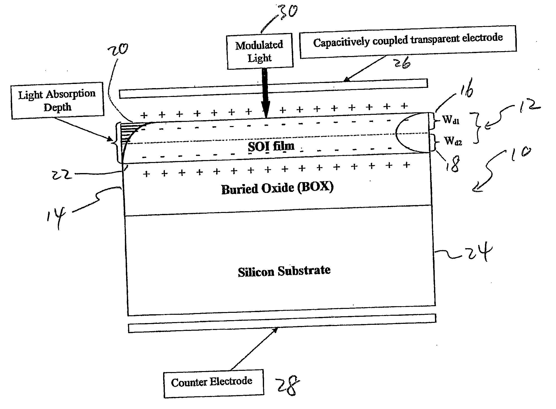
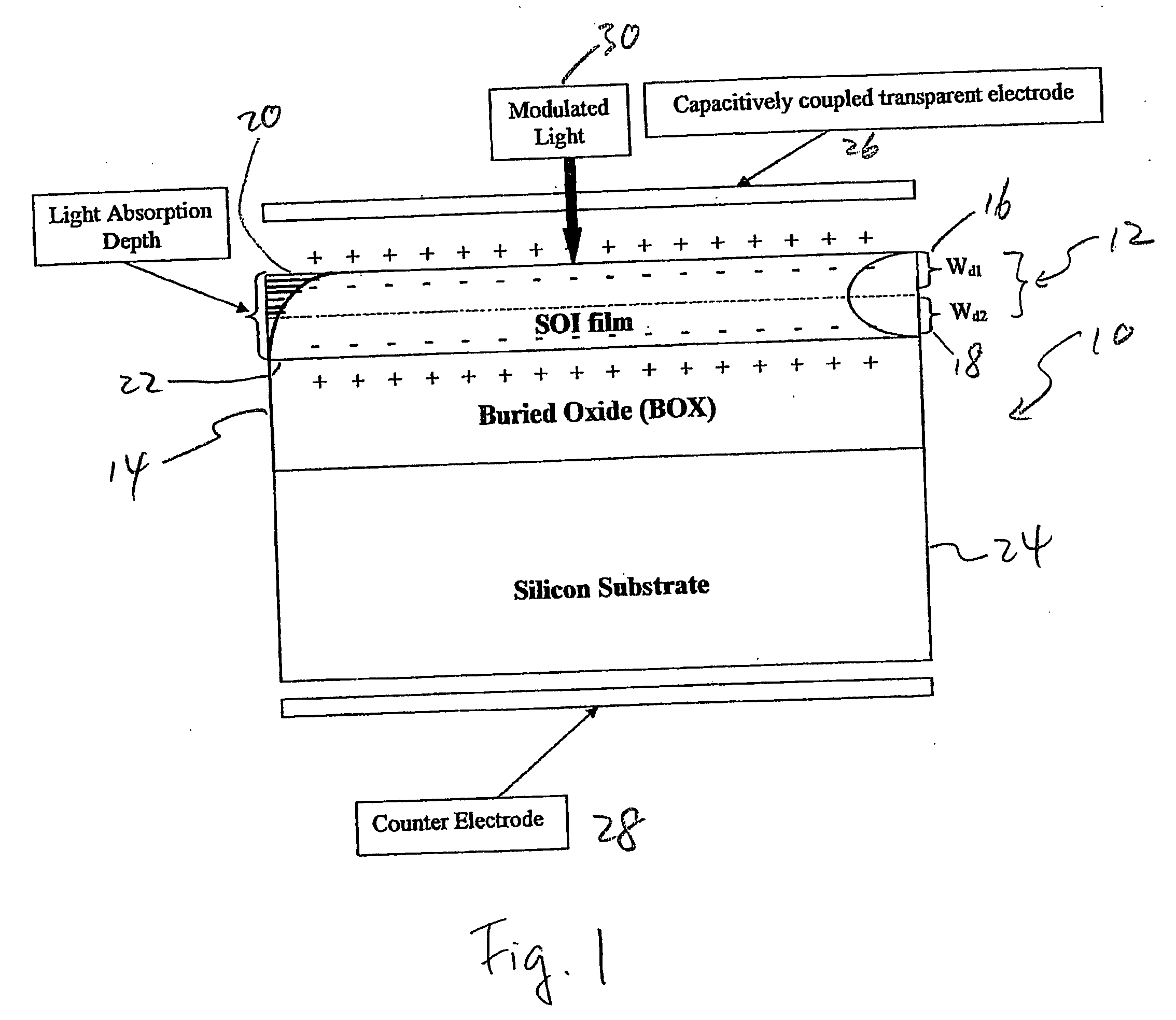
[0015] The invention relates to a method of measuring the thickness of the active silicon layer of a silicon-on-insulator structured wafer using a sub-surface photovoltage technique in the accumulation regime. The accumulation regime refers to the state that occurs when a voltage of opposite polarity is applied to a portion of a wafer to attract charges into a region. In depletion m...


PUM


Abstract

A method and apparatus for thickness measurement of an active layer of a silicon-on-insulator material comprising a layered structure of silicon film, a buried oxide layer and a silicon substrate. In one embodiment, the method comprises the steps of directing a low intensity light of an energy greater than the silicon band-gap on the silicon film, the energy of light sufficient to be substantially absorbed within the silicon film such that the error from the substrate excitation is small compared to the small signal calibration of the apparatus; modifying the surface potential with the chemical treatment, electrical bias or corona, measuring surface photovoltage of the silicon film; and calculating the thickness of the silicon film in response to a non-contact photovoltage measurement of the semiconductor layered structure.

Description

RELATED APPLICATIONS [0001] This application claims priority to and the benefit of U.S. provisional patent application Nos. 60 / 838,616, filed on Aug. 18, 2006, and 60 / 880,855, filed on Jan. 17, 2007, the entire disclosures of which are incorporated by reference herein.FIELD OF THE INVENTION [0002] The invention relates to a method of characterizing silicon-on-insulator material, and specifically to a method of measuring the thickness of a silicon-on-insulator (SOI) layer using a sub-surface photovoltage (PV). BACKGROUND OF THE INVENTION [0003] In modern silicon-on-insulator (SOI) based devices, two parameters are considered as the most critical: the silicon film thickness and the buried oxide (BOX) / silicon film interface defectiveness. Their accurate determination is especially important for the ultra-thin fully depleted SOI when the transistor threshold voltage is linked to the SOI thickness. Therefore, the main challenge for SOI metrology is a precise control of a silicon film thi...

Claims


Application Information

Patent Timeline
IPC IPC(8): G01J1/42
CPCG01B7/06H01L22/12G01B11/0625
Inventor TSIDILKOVSKI, EDWARDSTEEPLES, KENNETH
Owner SEMILAB SEMICON PHYSICS LAB
Why Eureka
Try Eureka