

Semiconductor memory device where write and read disturbances have been improved
a memory device and micro-conductor technology, applied in the direction of information storage, static storage, digital storage, etc., can solve the problems of destroying data, writing disturbance and reading disturbance, and increasing the variation of the threshold value of the transistor,
- Summary
- Abstract
- Description
- Claims
- Application Information
AI Technical Summary
Problems solved by technology
Method used
Image

Examples
first embodiment
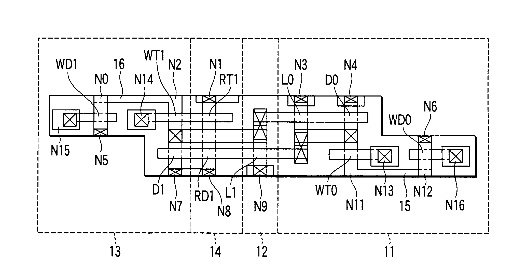
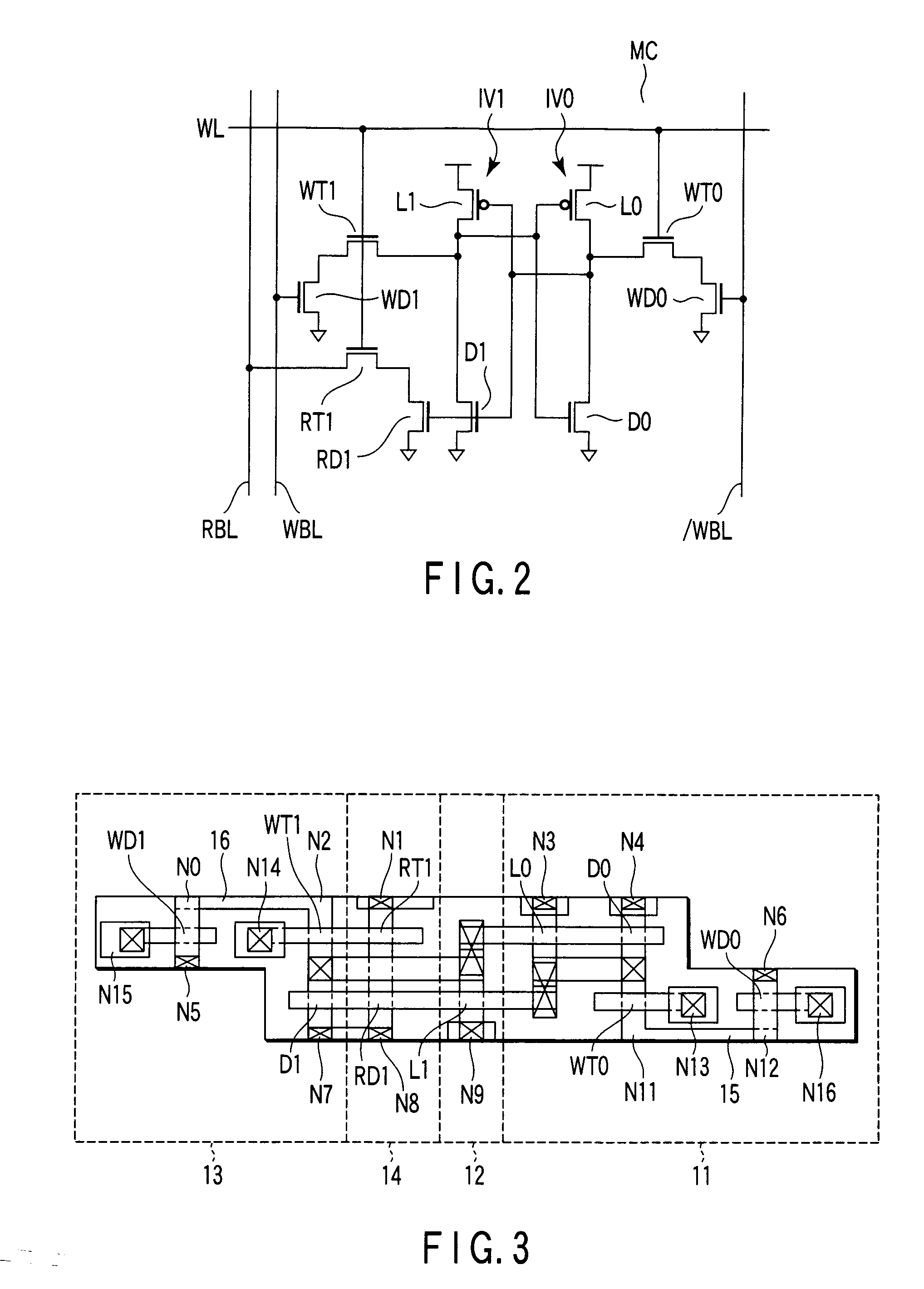
[0038]FIG. 3 schematically shows the layout of the memory cell of FIG. 2. FIG. 3 shows the source region / drain region / gate region (active area), polysilicon interconnect, contacts, metal interconnects, and others of a transistor formed on a semiconductor substrate. As shown in FIG. 3, transistors L0, D0, WT0, WD0 are arranged in a first area 11 on the semiconductor substrate. A transistor L1 is arranged a second area 12 adjacent to the first area 11. Moreover, transistors D1, WT1, and WD1 are arranged in a third area 13. Transistor RT1 and transistor RD1 are arranged in a fourth area 14 located between the second area 12 and the third area 13.
[0039]The other of the source and drain regions of the transistor WT0 and one of the source and drain regions of the transistor WD0 are connected to each other via a diffusion layer 15 arranged in the first area 11 on the semiconductor substrate. Similarly, the other of the source and drain regions of the transistor WT1 and one of the source an...
second embodiment
[0045]In the first embodiment, since data is read onto a single bit line RBL when data is read from each memory cell, this is effective when the number of memory cells connected to a bit line RBL is small. However, as the number of memory cells connected to a bit line RBL increases, a differential method may be effective in reading data.
[0046]FIG. 6 is a circuit diagram of a semiconductor memory device according to a second embodiment of the invention. FIG. 7 shows a memory cell in the memory cell array of FIG. 6.
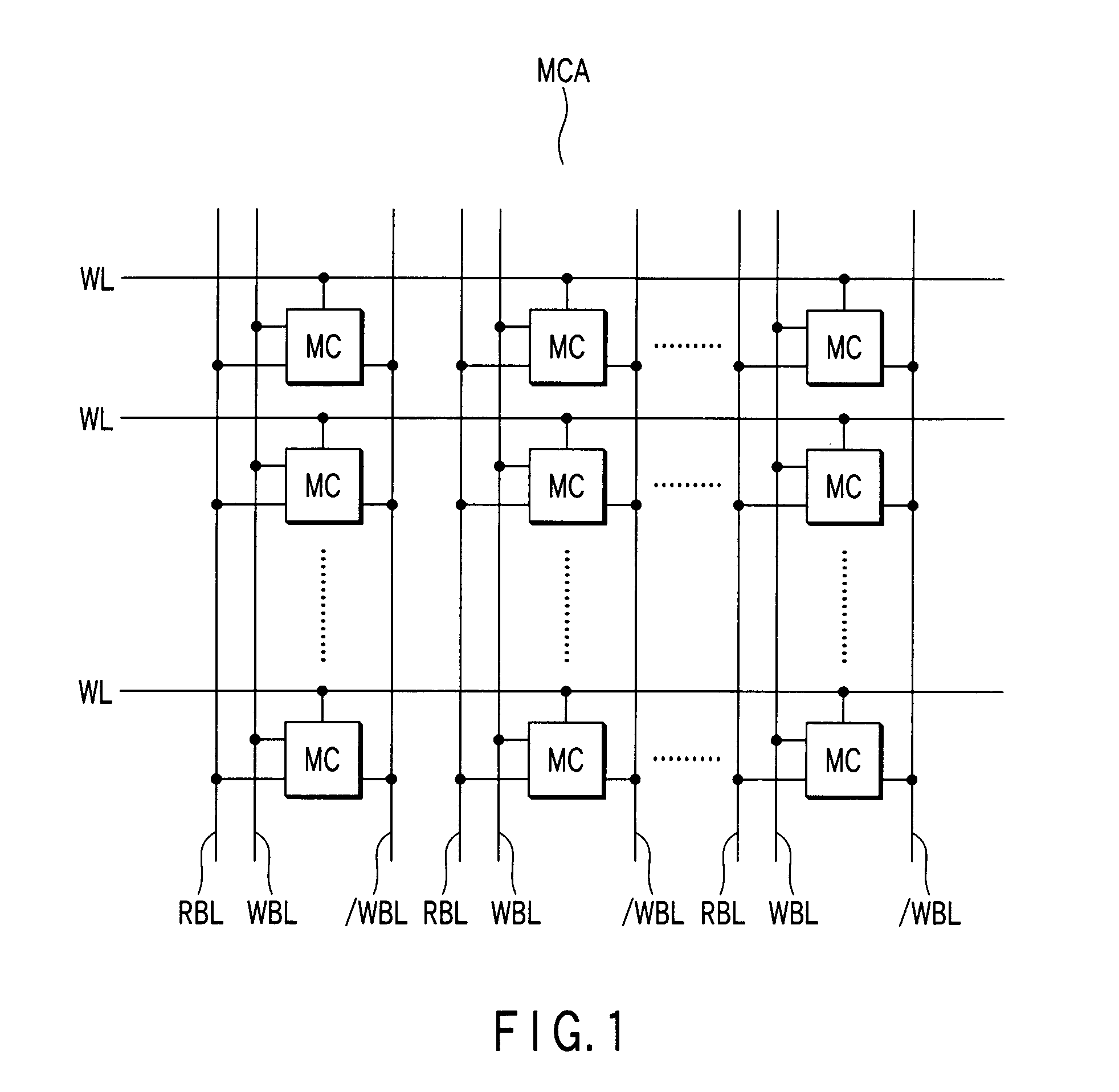
[0047]As shown in FIG. 6, there is provided a memory cell array MCA which has a plurality of memory cells MC arranged in a matrix. There are provided a plurality of word lines WL and a plurality of bit lines. The plurality of bit lines include two types of bit lines: data writing complementary bit lines WBL, / WBL and data reading complementary bit lines RBL, / RBL.
[0048]Each of the plurality of word lines WL is connected to a plurality of memory cells MC in each row of the m...
PUM
 Abstract
Description
Claims
Application Information