Semiconductor Memory Device, Rewrite Processing Method Therefor, and Program Thereof
- Summary
- Abstract
- Description
- Claims
- Application Information
AI Technical Summary
Benefits of technology
Problems solved by technology
Method used
Image
Examples
first embodiment
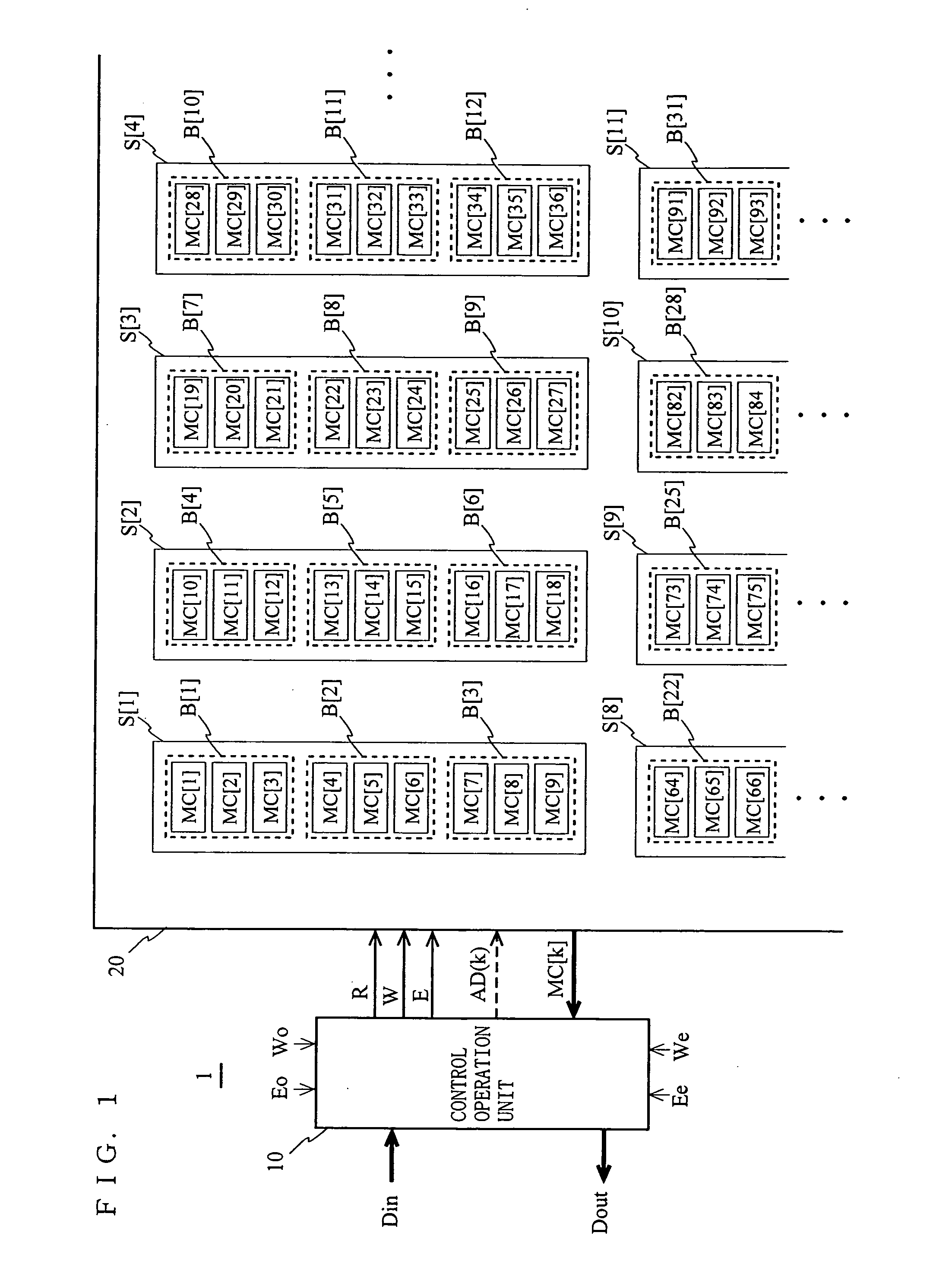
[0057]FIG. 1 is a block diagram of a semiconductor memory device 1 according to a first embodiment of the present invention. The semiconductor memory device 1 includes a control operation unit 10 and a memory body 20.
[0058] The memory body 20 includes a plurality of nonvolatile 1-bit storage memory cells MC[k] (k is a natural number) which are capable of continuing to hold stored data even after power has been turned off. In this embodiment, an explanation will be made based on the premise that the memory cells MC[k] are flash memory cells, each of which has a source electrode, a drain electrode, a floating gate and a gate electrode on a semiconductor substrate. And further, it is premised that a stored value, which is provided when the amount of electrons accumulated in the floating gate is equal to or larger than a predetermined amount, is 0, and a stored value, which is provided when the amount of electrons accumulated in the floating gate is smaller than the predetermined amoun...
third embodiment
[0122]FIG. 10 is a block diagram of a semiconductor memory device 3 according to a third embodiment of the invention. The semiconductor memory device 3 includes a control operation unit 10b and a memory body 20b.
[0123] The memory body 20b includes a plurality of nonvolatile 1-bit storage memory cells MC[k] (k is a natural number) that are capable of continuing to hold stored data even after power has been turned off. The present embodiment under the assumption that the memory body 20b is a flash memory as in the case of those described in the first and second embodiments. Although not shown in FIG. 10, the memory cells MC[k] are arranged in the memory cell arrangement region of the memory body 20b in the form of a matrix.
[0124] The data storage units B[m] (m is a natural number) each includes five memory cells MC[k]. In the semiconductor memory device 3 according to the present embodiment, the control of gate voltage is not exercised sector by sector and erasing is performed memor...
fourth embodiment
[0144]FIG. 12 is a block diagram of a semiconductor memory device provided with a program for executing the same processes as those performed by the semiconductor memory device described in the first embodiment. The semiconductor memory device according to the fourth embodiment includes a CPU 30, a storage unit 40, and the memory body 20b. The CPU 30 and the memory body 20b are coupled with each other by using a piece of hardware or a connecting status therebetween can be changed via a FPGA (field programmable gate array). The memory body 20b is the same as that described in the first embodiment and therefore, its detail description will be omitted. An address AD(k) is given to the memory cell MC[k] included in the memory body 20b.
[0145] The storage unit 40 is a memory, which is not rewritten, for storing a control operation program and control data to which the CPU 30 refers when rewriting data stored in the memory body 20b. In this case, the control operation program includes a r...
PUM
 Abstract
Description
Claims
Application Information


