Method of manufacturing a single chip semiconductor integrated circuit device including a mask ROM in a short time

Inactive Publication Date: 2008-02-28
MITSUMI ELECTRIC CO LTD
View PDF11 Cites 11 Cited by
  • Summary
  • Abstract
  • Description
  • Claims
  • Application Information

AI Technical Summary

Benefits of technology

[0026]It is therefore an exemplary object of the present invention to provide a method which is capable of manufactu

Problems solved by technology

However, at this time instance, the ultimate program has yet to be written in the mask ROM of the actual microcontroller.
As a result, the conventional method is disadvantageous in that it takes very much time (e.g. one year or one and half years) to develop the microcontroller as the ultimate product.
However, the product of the OTP version and the product of the mask ROM version are different from each other as semiconductor chips and cannot be compatible in characteristics in abund

Method used


Image

  • Method of manufacturing a single chip semiconductor integrated circuit device including a mask ROM in a short time
  • Method of manufacturing a single chip semiconductor integrated circuit device including a mask ROM in a short time
  • Method of manufacturing a single chip semiconductor integrated circuit device including a mask ROM in a short time

Examples


Embodiment Construction

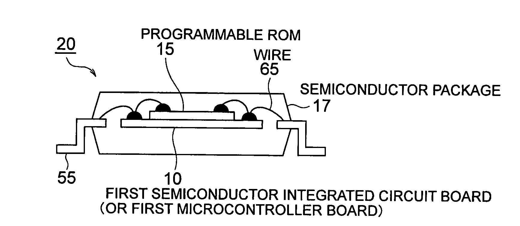
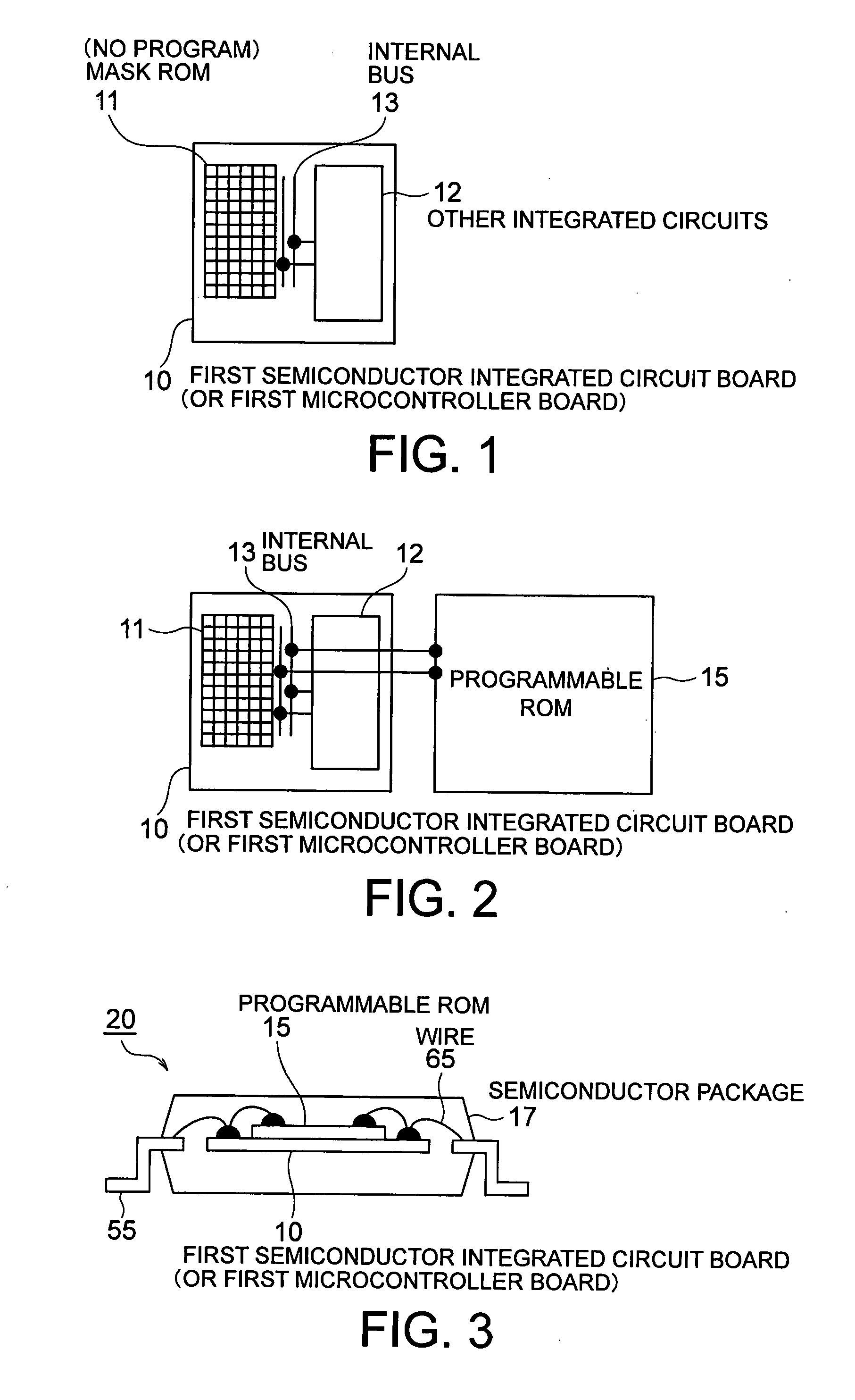
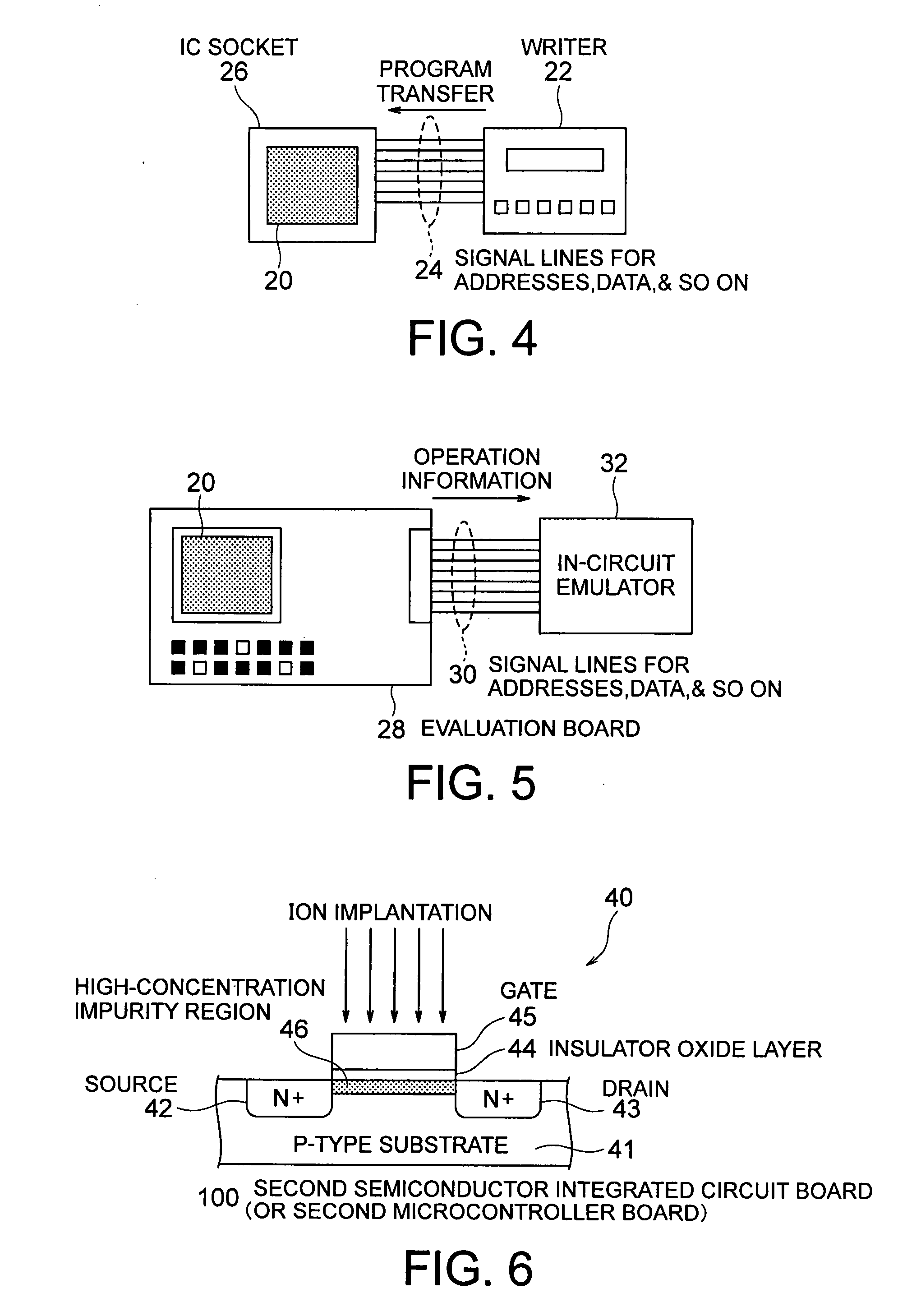
[0063]Referring to FIGS. 1 through 7, the description will proceed to a method of manufacturing a microcontroller according to an exemplary embodiment of this invention. Herein, in the manner which is described above, development of hardware of the microcontroller is carried out by a semiconductor maker side while development of software (a program) of the microcontroller is carried out by a user side. That is, development of the microcontroller is carried out in collaboration with the semiconductor maker and the user. In addition, the microcontroller to be manufactured as an ultimate product is one where an ultimate program is stored in a mask read only memory (ROM) and is a kind of single chip semiconductor integrated circuit devices.

[0064]First, between the semiconductor maker and the user, the discussions of specification of the microcontroller (the single chip semiconductor integrated circuit device) to be manufactured are carried out. Herein, an ultimate microcontroller to be ...


PUM


Abstract

In a state of a first semiconductor integrated circuit device on which a first semiconductor integrated circuit board including a first mask ROM and a programmable ROM are mounted, an ultimate program determined by using the programmable ROM is stored in a second ROM of a second semiconductor integrated circuit board which is substantially similar in structure to the first semiconductor integrated circuit board, thereby manufacturing a second semiconductor integrated circuit device as an ultimate product.

Description

[0001]This application is based upon and claims the benefit of priority from Japanese patent application No. 2006-207797, filed on Jul. 31, 2006, the disclosure of which is incorporated herein its entirety by reference.BACKGROUND OF THE INVENTION[0002]This invention relates to a method of manufacturing a single chip semiconductor integrated circuit device (a microcontroller) and a method of debugging a program of the single chip semiconductor integrated circuit device.[0003]As well know in the art, a microcomputer is defined by a miniaturized electronic computer constituted by a microprocessor. The microprocessor is a processor wherein a central processing unit (CPU) of the computer is integrated on one or few large-scale integrated circuits (LSIs). The microcomputer normally comprises the CPU, an input / output device, and a main memory device. The main memory device comprises a random access memory (RAM) and a read only memory (ROM). An input / output control LSI is used as a connecti...

Claims


Application Information

Patent Timeline
IPC IPC(8): H01L21/77
CPCH01L23/49575H01L23/50H01L2924/1306H01L2924/13091H01L2924/014H01L2924/01033H01L2924/01006H01L24/48H01L2924/14H01L2924/01082H01L24/49H01L25/0657H01L27/0207H01L27/105H01L27/112H01L27/11293H01L2223/5444H01L2224/16H01L2224/32145H01L2224/48091H01L2224/48137H01L2224/48145H01L2224/48247H01L2224/4911H01L2224/49171H01L2225/06506H01L2225/0651H01L2924/01004H01L2924/01005H01L2924/01013H01L2924/01015H01L2924/01047H01L2924/01075H01L2924/00014H01L2924/00H01L2224/05554H01L2224/451H01L2924/181H01L2224/05599H01L2224/85399H01L2924/10161H01L2924/10162H10B20/65H10B20/00H01L2224/45015H01L2924/207H01L2924/00012H01L2224/45099H01L25/065H01L25/07H01L25/18
Inventor YANO, KOJISEGAWA, TOMOKI
Owner MITSUMI ELECTRIC CO LTD
Why Eureka
Try Eureka