Method of manufacturing a stamper

a stamper and manufacturing method technology, applied in the field of manufacturing methods of stampers, can solve the problems of high cost, long processing time, and degraded product reliability, and achieve the effects of reducing the cost of production, and reducing the quality of production

Inactive Publication Date: 2008-03-06
SAMSUNG ELECTRO MECHANICS CO LTD
View PDF1 Cites 126 Cited by
  • Summary
  • Abstract
  • Description
  • Claims
  • Application Information

AI Technical Summary

Benefits of technology

[0015]An aspect of the invention is to provide a method of manufacturing a broad stampe

Problems solved by technology

However, manufacturing a board using the UV lithography method may have the limitations that the copper foil must be thick and that wet etching must be used, whereby the reliability of the products may be degraded when using UV lithography to form fine patterns with a pitch

Method used


Image

  • Method of manufacturing a stamper
  • Method of manufacturing a stamper
  • Method of manufacturing a stamper

Examples


Embodiment Construction

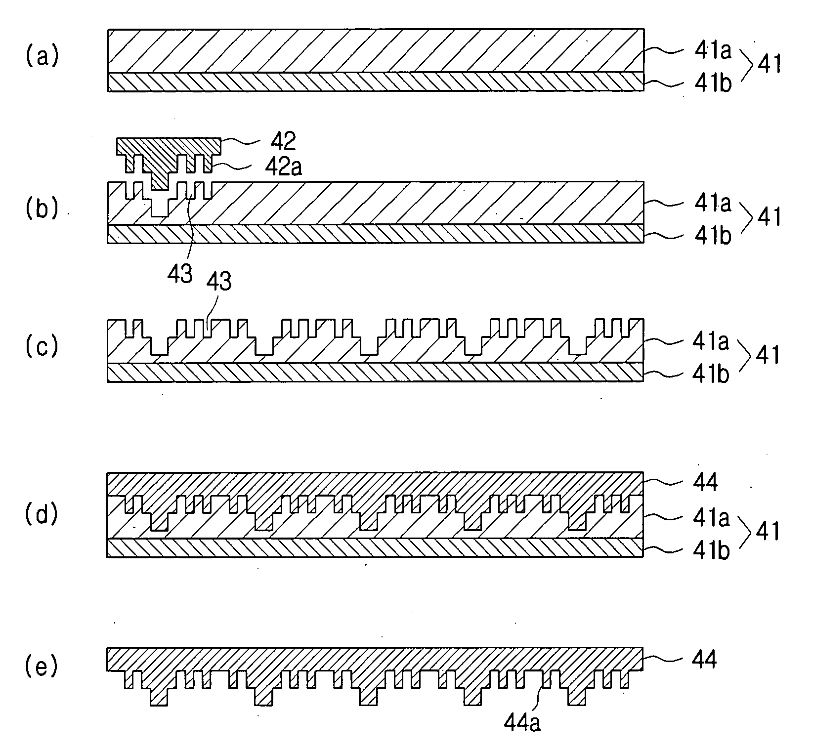
[0027]The method of manufacturing a stamper according to certain embodiments of the invention will be described below in more detail with reference to the accompanying drawings, in which those components are rendered the same reference numeral that are the same or are in correspondence, regardless of the figure number, and redundant explanations are omitted.

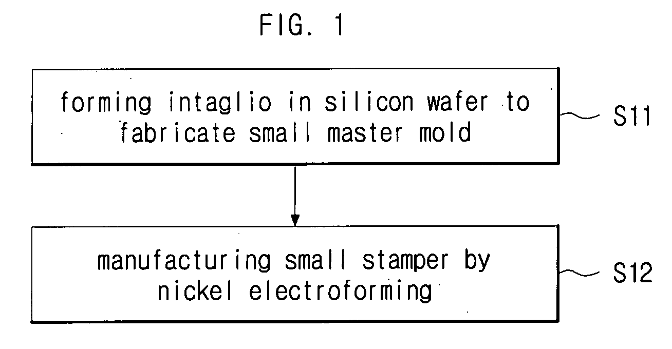
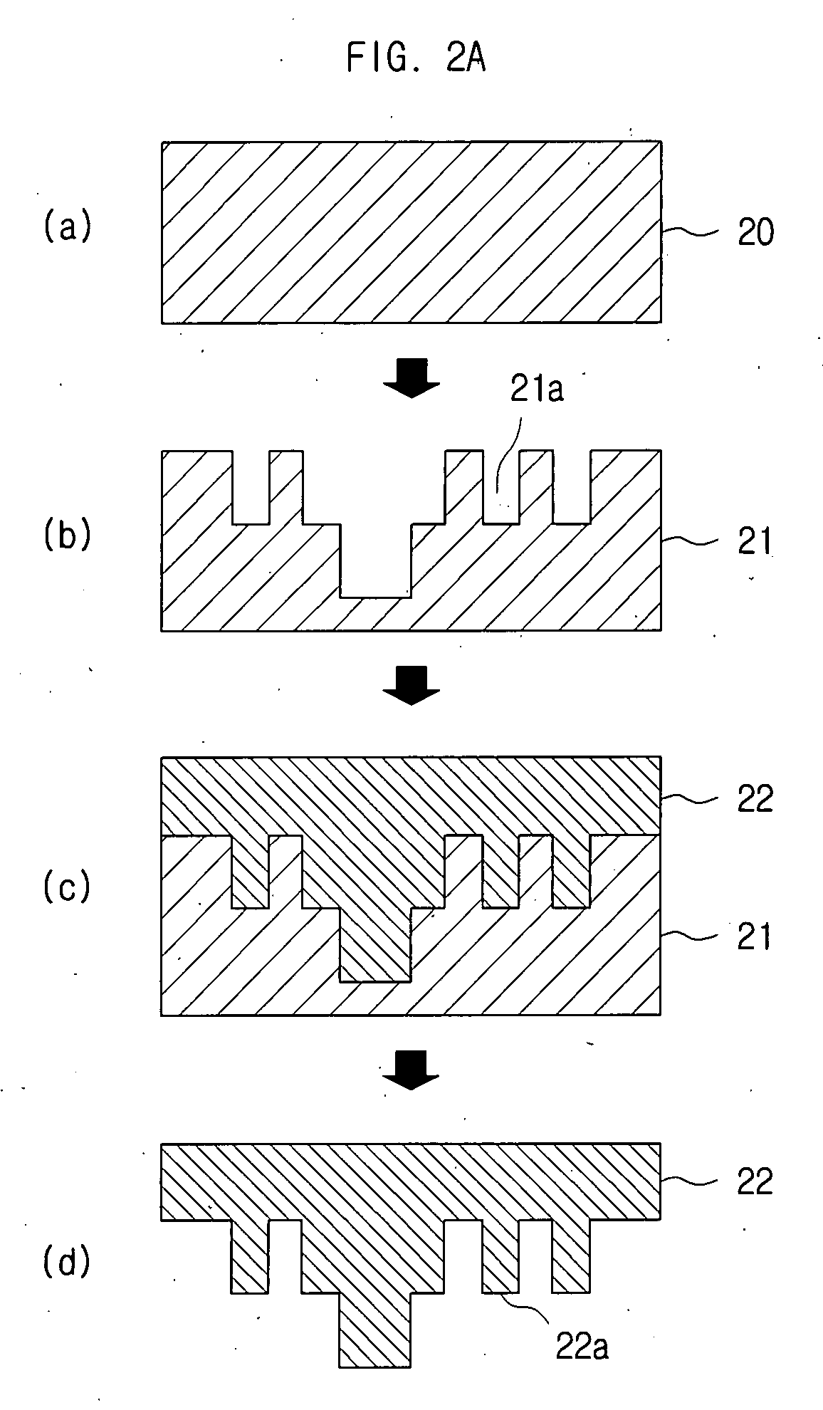
[0028]FIG. 1 is a flowchart of a process for manufacturing a small stamper according to a first disclosed embodiment of the invention, and FIG. 2a is a flow diagram of a process for manufacturing a small stamper according to the first disclosed embodiment of the invention. In FIG. 2a are illustrated a silicon wafer 20, a small master mold 21, an intaglio 21a, a small stamper 22, and a relievo 22a.

[0029]Operation S11 of FIG. 1 may be to form the intaglio 21a in the silicon wafer 20 to fabricate the small master mold 21, where drawings (a) and (b) of FIG. 2 represent the corresponding processes. The method of forming the intaglio ...


PUM


Abstract

A method of manufacturing a stamper is disclosed. By using a method that includes: manufacturing a small stamper, in which a first relievo is formed; repeatedly imprinting the small stamper on a large master mold to form a first intaglio corresponding to the first relievo; and molding such that a second relievo is formed, which is in correspondence with the first intaglio, a broad stamper having identical repeated patterns may be manufactured.

Description

CROSS-REFERENCE TO RELATED APPLICATIONS[0001]This application claims the benefit of Korean Patent Application No. 10-2006-0083305 filed with the Korean Intellectual Property Office on Aug. 31, 2006, the disclosure of which is incorporated herein by reference in its entirety.BACKGROUND[0002]1. Technical Field[0003]The present invention relates to a method of manufacturing a stamper, more particularly to a method of manufacturing a broad stamper which has the same patterns repeated.[0004]2. Description of the Related Art[0005]In step with the societal demands of the twenty first century for high-tech information and communication, electronics and electrical technology has seen rapid advances towards greater storage capacities, faster information processing and transmission, and more convenient information communication networks.[0006]In particular, under the condition of finiteness in information transmission speeds, the method is being suggested of generating new functionalities by i...

Claims


Application Information

Patent Timeline
IPC IPC(8): B29C33/38
CPCB29C33/3878H05K2203/0108H05K3/0014G03F7/0002H05K3/1258
Inventor RA, SEUNG-HYUNHONG, MYEONG-HOLEE, HYUK-SOOLEE, JUNG-WOOKWAK, JEONG-BOK
Owner SAMSUNG ELECTRO MECHANICS CO LTD
Why Eureka
Try Eureka